Digital characteristics, Switching characteristics, Ds261pp5 – Cirrus Logic CS61584A User Manual
Page 8
CS61584A
8
DS261PP5
DS261PP5
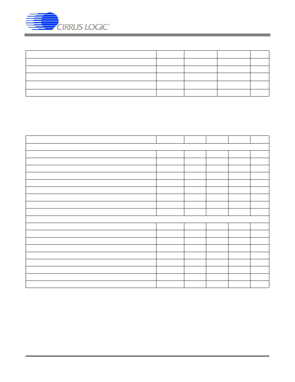
DIGITAL CHARACTERISTICS
(T
A
= -40 to 85 °C; power supply pins within ±5% of nominal.)
Notes: 23. Digital inputs are designed for CMOS logic levels.
24. Digital outputs are TTL compatible and drive CMOS levels into a CMOS load.
SWITCHING CHARACTERISTICS
(T
A
= -40 to 85 °C; power supply pins within ±5% of nominal;
Inputs: Logic 0 = 0 V, Logic 1 = DV+.)
Notes: 25. The maximum burst rate of a gapped TCLK input clock is 8.192 MHz. For the gapped clock to be
tolerated by the CS61584A, the jitter attenuator must be switched to the transmit path of the line
interface. The maximum gap size that can be tolerated on TCLK is 28 UIp-p.
26. RCLK duty cycle may be outside the specified limits when the jitter attenuator is in the transmit path
and when the jitter attenuator is employing the overflow/underflow protection mechanism.
27. At max load of 50 pF.
Parameter
Symbol
Min
Max
Unit
High-Level Input Voltage
(Note 23)
V
IH
(DV+) - 0.5
-
V
Low-Level Input Voltage
(Note 23)
V
IL
-
0.5
V
High-Level Output Voltage (I
out
= -40 µA)
(Note 24)
V
OH
(DV+) - 0.3
-
V
Low-Level Output Voltage (I
out
= 1.6 mA)
(Note 24)
V
OL
-
0.3
V
Input Leakage Current (Digital pins except J-TMS and J-TDI)
-
±10
µA
Parameter
Symbol
Min
Typ
Max
Unit
T1 Clock/Data
TCLK Frequency
(Note 25)
f
tclk
-
1.544
-
MHz
TCLK Duty Cycle
t
pwh2
/t
pw2
20
50
80
%
RCLK Duty Cycle
(Note 26)
t
pwh1
/t
pw1
45
50
55
%
Rise Time (All Digital Outputs)
(Note 27)
t
r
-
-
65
ns
Fall Time (All Digital Outputs)
(Note 27)
t
f
-
-
65
ns
RPOS/RNEG (RDATA) to RCLK Rising Setup Time
t
su1
-
274
-
ns
RCLK Rising to RPOS/RNEG (RDATA) Hold Time
t
h1
-
274
-
ns
TPOS/TNEG (TDATA) to TCLK Falling Setup Time
t
su2
25
-
-
ns
TCLK Falling to TPOS/TNEG (TDATA) Hold Time
t
h2
25
-
-
ns
E1 Clock/Data
TCLK Frequency
(Note 25)
f
tclk
-
2.048
-
MHz
TCLK Duty Cycle
t
pwh2
/t
pw2
20
50
80
%
RCLK Duty Cycle
(Note 26)
t
pwh1
/t
pw1
45
50
55
%
Rise Time (All Digital Outputs)
(Note 27)
t
r
-
-
65
ns
Fall Time (All Digital Outputs)
(Note 27)
t
f
-
-
65
ns
RPOS/RNEG (RDATA) to RCLK Rising Setup Time
t
su1
-
194
-
ns
RCLK Rising to RPOS/RNEG (RDATA) Hold Time
t
h1
-
194
-
ns
TPOS/TNEG (TDATA) to TCLK Falling Setup Time
t
su2
25
-
-
ns
TCLK Falling to TPOS/TNEG (TDATA) Hold Time
t
h2
25
-
-
ns
CS61584A
8
DS261F1