Applications, Figure 27. hardware mode configuration, Table 13. cs61584a external components – Cirrus Logic CS61584A User Manual
Page 48: 1 line interface, Ds261pp5, Applications 13.1 line interface
CS61584A
48
DS261PP5
DS261PP5
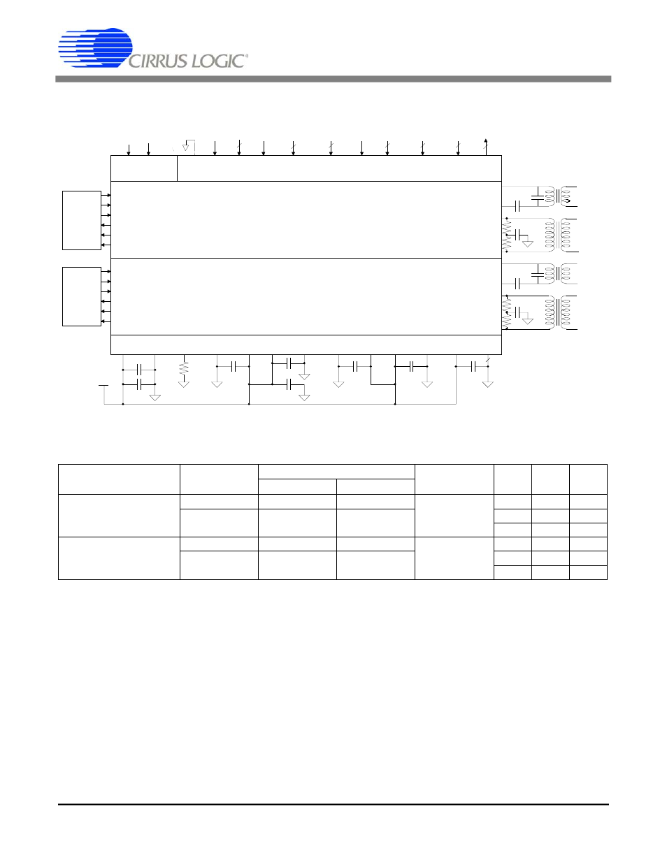
13. APPLICATIONS
13.1
Line Interface
Figures 27-29 illustrate typical connection diagram
for T1 and E1 line interface circuits in Hardware,
Host serial port, and Host parallel port modes. Ta-
ble 13 lists the external components that are re-
quired in T1 and E1 applications for both the 5.0
and 3.3 Volt devices.
In the transmit line interface circuitry, capacitors
C1 and C2 provide transmitter return loss. The
0.47 µF capacitor in series with the transformer pri-
mary prevents output stage imbalances from pro-
ducing a DC current through the transformer that
might saturate the transformer and result in an out-
put level offset.
In the receive line interface circuitry, resistors R1-
R4 provide receive impedance matching and re-
ceiver return loss. The 0.47 µF capacitor to ground
provides the necessary differential input voltage
reference for the receiver.
Device Suffix
Data Rate
(MHz)
REFCLK Frequency (MHz)
Transformer
Turns Ratio
Cable
(
Ω
)
R1-R4
(
Ω
)
C1-C2
(pF)
1XCLK = 1
1XCLK = 0
-IL3 and -IQ3 (3.3 Volts)
1.544
1.544
12.352
1:2
100
12.4
560
2.048
2.048
16.384
75
9.31
2200
120
15.0
560
-IL5 and -IQ5 (5.0 Volts)
1.544
1.544
12.352
1:1.15
100
38.3
220
2.048
2.048
16.384
75
28.7
470
120
45.3
220
Table 13. CS61584A External Components
AV+
AGND
BGREF
TV+1
TGND1
RV+1
RGND1 DV+ DGND1:3
0.01
µ
F
TCLK1
TPOS1
TNEG1
RCLK1
RPOS1
RNEG1
TCLK2
TPOS2
TNEG2
RCLK2
RPOS2
RNEG2
Framer
Framer
TTIP1
TRING1
RTIP1
RRING1
TTIP2
TRING2
RTIP2
RRING2
Hardware Control
Power Supply
Clock Generator
Channel 2
Channel 1
transmit
transmit
3
0.1
µ
F
1
µ
F
+
0.1
µ
F
TV+2
TGND2
RV+2
RGND2
22
µ
F
+
0.1
µ
F
0.1
µ
F
0.1
µ
F
receive
R3
R4
receive
R1
R2
T1
T2
T3
T4
R3
4.99k
Ω
V
CC
0.47
µ
F
0.47
µ
F
REFCLK 1XCLK
RESET
CLKE
TAOS[1:2]
RLOOP[1:2] LLOOP
CON[0:2]1 CON[0:2]2
ATTEN[0:1]
C1
C2
0.47
µ
F
0.47
µ
F
LOS[1:2]
PD[1:2]
MODE
2
3
2
2
3
2
2
1:N
1:N
1:N
1:N
Figure 27. Hardware Mode Configuration
CS61584A
48
DS261F1