3 control a registers, Table 7. control a registers, Ds261pp5 – Cirrus Logic CS61584A User Manual
Page 26
CS61584A
26
DS261PP5
DS261PP5
AAO: The Automatic All-Ones (AAO) bit in the
Mask Register (Channel 1, bit 1) causes an un-
framed all-ones pattern to be output at the RPOS
and RNEG (or RDATA) pins when the receiver is
in a loss of signal (LOS) condition.
9.1.3
Control A Registers
The Control A registers are read-write registers and
are shown in Table 7. The Control A registers se-
lect device configuration and power down control.
CLKE: Establishes the edge of the of RCLK that
RPOS and RNEG (or RDATA) are valid.
PD: Controls per channel power down.
ATTEN0 and ATTEN1: Controls the jitter attenu-
ator location and -3 dB knee frequency (See Jitter
Attenuator section).
CODER: Controls the coder mode function. The
TPOS, TNEG, RPOS, and RNEG pins are active
when the transparent mode is enabled. The TDA-
TA, RDATA, AIS, and BPV pins are active when
the coder mode is enabled.
AMI-T: Controls the line encoder in the transmit
direction. The selection of B8ZS or HDB3 is deter-
mined by the CON[3:0] bits (See the Transmitter
section).
AMI-R: Controls the line decoder in the receive di-
rection. The selection of B8ZS or HDB3 is deter-
mined by the CON[3:0] bits (See the Transmitter
section).
EXZ: Controls the automatic detection of excessive
zeros on the BPV pin according to ANSI T1.231
when coder mode is enabled (CODERx = 1).
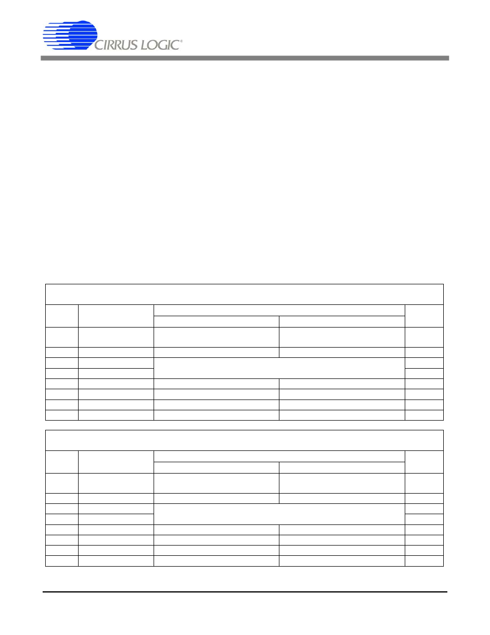
Control A Register (Channel 1)
Serial Port Address: 0x14; Parallel Port Address: 0xY4
Bit
Description
Definition
Reset
Value
1
0
7
CLKE
RPOS/RNEG (or RDATA) valid on
falling edge of RCLK
RPOS/RNEG (or RDATA) valid on
rising edge of RCLK
0
6
PD1
Power down channel
Power up channel
0
5
ATTEN01
Jitter attenuator location
(See Jitter Attenuator section)
0
4
ATTEN11
0
3
CODER1
Coder mode enabled
Transparent mode enabled
0
2
AMI-T1
AMI encoder enabled
B8ZS/HDB3 encoder enabled
0
1
AMI-R1
AMI decoder enabled
B8ZS/HDB3 decoder enabled
0
0
Factory Test
Test
Normal operation
0
Control A Register (Channel 2)
Serial Port Address: 0x15; Parallel Port Address: 0xY5
Bit
Description
Definition
Reset
Value
1
0
7
EXZ
Excessive zeros detection for both
channels enabled
Excessive zeros detection for both
channels disabled
0
6
PD2
Power down channel
Power up channel
0
5
ATTEN02
Jitter attenuator location
(See Jitter Attenuator section)
0
4
ATTEN12
0
3
CODER2
Coder mode enabled
Transparent mode enabled
0
2
AMI-T2
AMI encoder enabled
B8ZS/HDB3 encoder enabled
0
1
AMI-R2
AMI decoder enabled
B8ZS/HDB3 decoder enabled
0
0
Factory Test
Test
Normal operation
0
Table 7. Control A Registers
CS61584A
26
DS261F1