2 serial port operation, Figure 21. serial read/write format (spol = 0), Figure 22. address command byte – Cirrus Logic CS61584A User Manual
Page 30: Ds261pp5

CS61584A
30
DS261PP5
DS261PP5
9.2
Serial Port Operation
Serial port operation in Host mode is selected when
the MODE pin is set high and the P/S pin is set low.
In this mode, the CS61584A register set is accessed
by setting the chip select (CS) pin low and commu-
nicating over the SDI, SDO, and SCLK pins. Tim-
ing over the serial port is independent of the
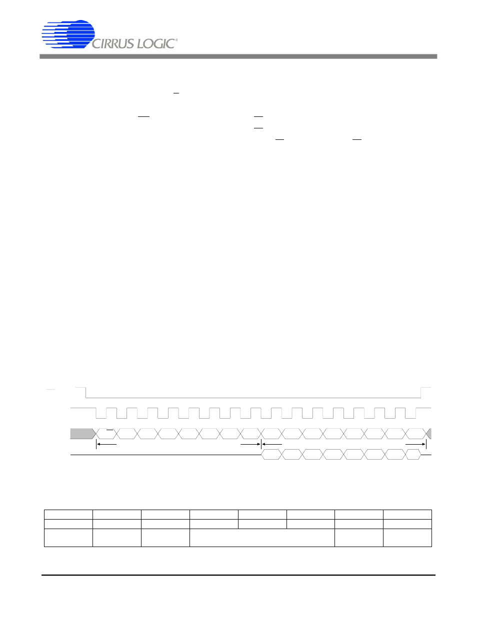
transmit and receive system timing. Figure 21 illus-
trates the format of serial port data transfers.
A read or write is initiated by writing an ad-
dress/command byte (ACB) to SDI. During a read
cycle, the register data addressed by the ACB is
output on SDO on the next eight SCLK clock cy-
cles. During a write cycle, the data byte immediate-
ly follows the ACB. A second address byte is
required when reading or writing the Arbitrary
Waveform registers (see below).
Data is written to and read from the serial port in
LSB first format. When writing to the port, SDI in-
put data is sampled by the device on the rising edge
of SCLK. The polarity of the data output on SDO is
controlled by the SPOL pin. When the SPOL pin is
low, data on SDO is valid on the rising edge of
SCLK. When the SPOL pin is high, data on SDO is
valid on the falling edge of SCLK. The SDO pin is
high impedance when not transmitting data. If the
host processor has a bi-directional I/O port, SDI
and SDO may be tied together.
As illustrated in Figure 22, the ACB consists of a
R/W bit, address field, and two reserved bits. The
R/W bit specifies if the current register access is a
read (R/W = 1) or a write (R/W = 0) operation. The
address field specifies the register address from
0x10 to 0x19. The reserved bit must be cleared for
normal operation of serial mode.
During register addressing, the first eight registers
are addressed as 0x10 to 0x17 in the address field
of the ACB. Because Arbitrary Waveform registers
0x18 and 0x19 access multiple bytes of RAM,
reading or writing these registers requires an Ad-
dress Command Byte followed by a RAM address
byte for each data transfer. The ACB specifies ei-
ther 0x18 or 0x19 in the address field to access the
channel 1 or channel 2 Arbitrary Waveform regis-
ter set. The RAM address is an 8-bit, unsigned bi-
nary number in the range of 0x00 to 0x29 to
identify one of 42 RAM locations. The data byte
containing the 7-bit, 2’s complement number spec-
ifying the phase amplitude completes the 24 SCLK
write cycle.
CS
SCLK
SDO
SDI
D6
D5
D4
D3
D2
D1
D0
D7
0
0
D7
D6
D5
D4
D3
D2
D1
D0
Address/Command Byte(s)
Data Output
0
0
0
1
0
R/W
Data Input
Figure 21. Serial Read/Write Format (SPOL = 0)
Figure 22. Address Command byte
B7 (MSB)
B6
B5
B4
B3
B2
B1
B0
Reserved
Reserved
ADR4
ADR3
ADR2
ADR1
ADR0
R/W
0
0
MSB
Address Field
LSB
0 = Write
1 = Read
CS61584A
30
DS261F1
