4 analog input, 5 output coding format, Table 1. output coding, two’s complement – Cirrus Logic CS5560 User Manual
Page 16: Table 2. output coding, offset binary, 4 analog input 3.5 output coding format, Cs5560
CS5560
16
DS713PP2
5/4/09
3.4 Analog Input
The analog input of the converter is fully differential with a peak-to-peak input of 4.096 volts on each input.
Therefore, the differential, peak-to-peak input is 8.192 volts. This is illustrated in
and
.
These diagrams also illustrate a differential buffer amplifier configuration for driving the CS5560.
The capacitors at the outputs of the amplifiers provide a charge reservoir for the dynamic current from the
A/D inputs while the resistors isolate the dynamic current from the amplifier. The amplifiers can be pow-
ered from higher supplies than those used by the A/D but precautions should be taken to ensure that the
op amp output voltage remains within the power supply limits of the A/D, especially under start-up condi-
tions.
3.5 Output Coding Format
The reference voltage directly defines the input voltage range in both the unipolar and bipolar configura-
tions. In the unipolar configuration (BP/UP low), the first code transition occurs 0.5 LSB above zero, and
the final code transition occurs 1.5 LSBs below VREF. In the bipolar configuration (BP/UP high), the first
code transition occurs 0.5 LSB above -VREF and the last transition occurs 1.5 LSBs below +VREF. See
for the output coding of the converter.
NOTE: VREF = (VREF+) - (VREF-)
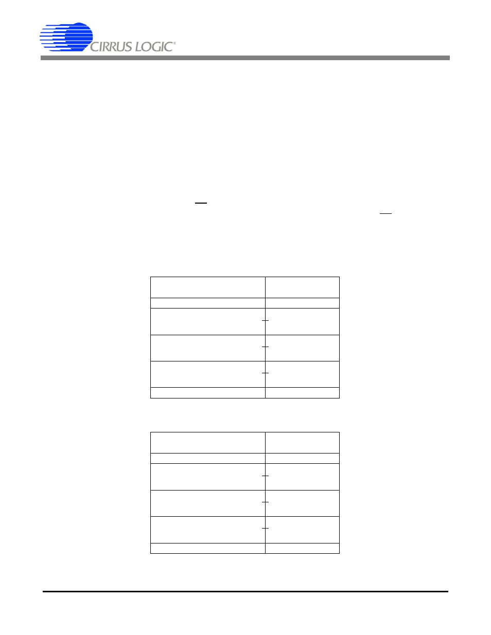
Table 1. Output Coding, Two’s Complement
Bipolar Input Voltage
Two’s
Complement
>(VREF-1.5 LSB)
7F FF FF
VREF-1.5 LSB
7F FF FF
7F FF FE
-0.5 LSB
00 00 00
FF FF FF
-VREF+0.5 LSB
80 00 01
80 00 00
<(-VREF+0.5 LSB)
80 00 00
NOTE: VREF = (VREF+) - (VREF-)
Table 2. Output Coding, Offset Binary
Unipolar Input Voltage
Offset
Binary
>(VREF-1.5 LSB)
FF FF FF
VREF-1.5 LSB
FF FF FF
FF FF FE
(VREF/2)-0.5 LSB
80 00 00
7F FF FF
+0.5 LSB
00 00 01
00 00 00
<(+0.5 LSB)
00 00 00