Hardware, 1 introduction, 2 evaluation board overview – Cirrus Logic CS5550 User Manual
Page 4: 1 analog section, Table 1. analog input selection, Cdb5550
CDB5550
4
1. HARDWARE
1.1 Introduction
The CDB5550 evaluation board provides a quick means of evaluating the CS5550 A/D converter. The
CDB5550 evaluation board’s analog section operates from a single +5 V power supply. The evaluation
board interfaces the CS5550 to an IBM
TM
compatible PC via a USB interface. To accomplish this, the
board comes equipped with a C8051F320 microcontroller and a USB connector which physically interfac-
es the evaluation board to the PC. Additionally, analysis software provides easy access to the internal
registers of the CS5550, and provides a means to display the performance in the time domain or frequen-
cy domain.
1.2 Evaluation Board Overview
The board is partitioned into two main sections: analog and digital. The analog section consists of the
CS5550, analog inputs, and an optional external voltage reference input. The digital section consists of
the microcontroller, interface header, reset circuitry, and the USB interface. The board also provides two
binding posts for easy power supply connectivity.
1.2.1 Analog Section
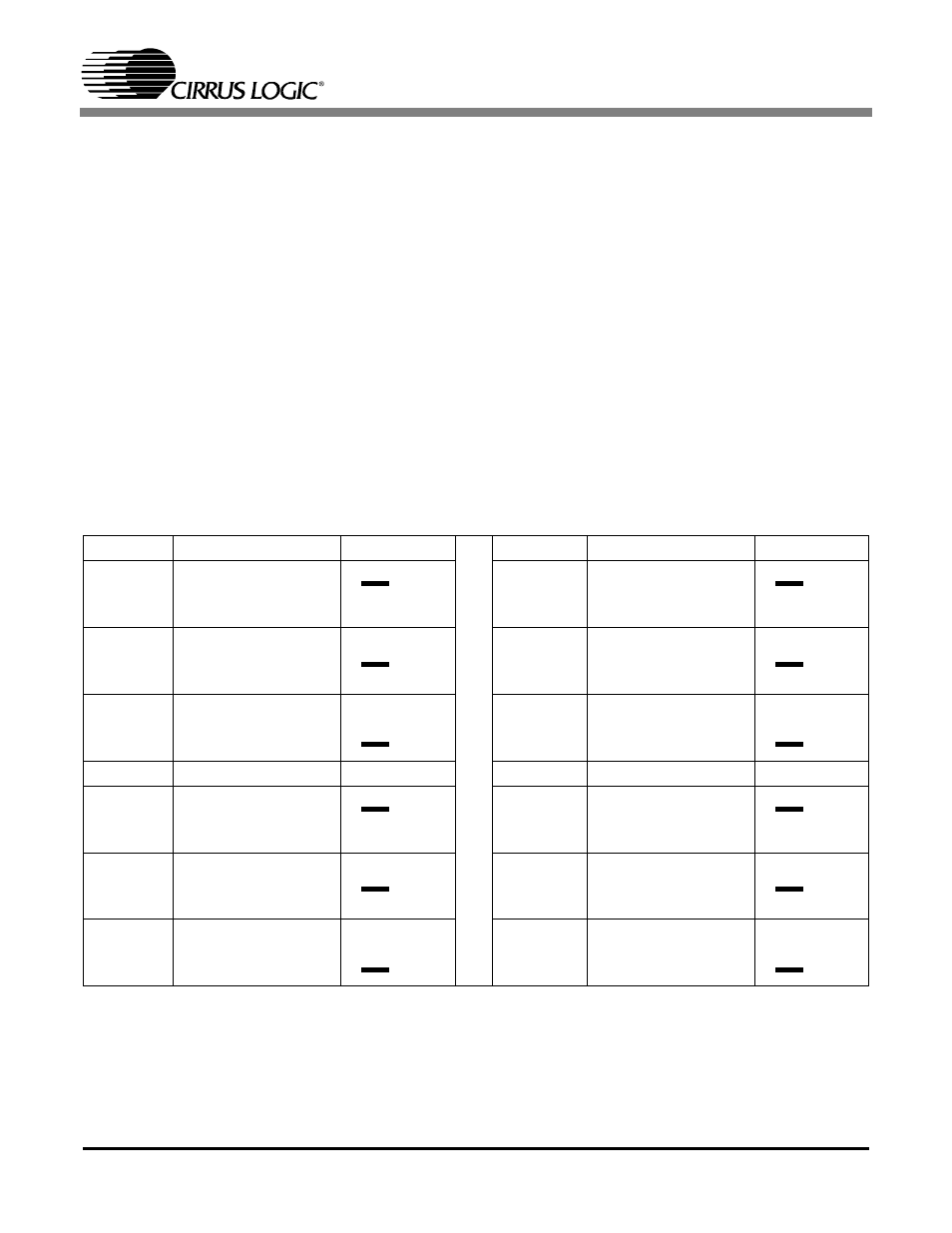
The CDB5550 provides several options for driving the analog inputs into the converter. These options in-
clude an external analog source, the voltage reference, and ground. Refer to Table 1.
The external analog inputs also provide +5 V and ground connectors which can be used to power a load
cell.
Reference
Description
J11
Reference
Description
J5
AIN1+
Selects the external
analog input (J13)
AIN2+
Selects the external
analog input (J10)
VREF
Selects the voltage ref-
erence sourced from
J7
VREF
Selects the voltage ref-
erence sourced from
J7
GND
Selects the ground
reference
GND
Selects the ground
reference
Reference
Description
J14
Reference
Description
J9
AIN1-
Selects the external
analog input (J13)
AIN2-
Selects the external
analog input (J10)
VREF
Selects the voltage ref-
erence sourced from
J7
VREF
Selects the voltage ref-
erence sourced from
J7
GND
Selects the ground
reference
GND
Selects the ground
reference
Table 1. Analog Input Selection
O O AIN1+
O O VREF
O O GND
O O AIN2+
O O VREF
O O GND
O O AIN1+
O O VREF
O O GND
O O AIN2+
O O VREF
O O GND
O O AIN1+
O O VREF
O O GND
O O AIN2+
O O VREF
O O GND
O O AIN1-
O O VREF
O O GND
O O AIN2-
O O VREF
O O GND
O O AIN1-
O O VREF
O O GND
O O AIN2-
O O VREF
O O GND
O O AIN1-
O O VREF
O O GND
O O AIN2-
O O VREF
O O GND