An150 – Cirrus Logic AN150 User Manual
Page 3
AN150
AN150REV2
3
number of bits in the output word (16 for the
CS5531/33 and 24 for CS5532/34).
Example: Using the CS5532 in the 64X unipolar
range with a 2.5V reference and the gain register
set to 1.0, V
SPAN
is nominally 39.0625 mV, and N
is 24. The size of one LSB is then equal to 39.0625
mV / 2^24, or approximately 2.328 nV.
The output coding for both the 16-bit and 24-bit
parts depends on whether the device is used in uni-
polar or bipolar mode, as shown in Table 1. In uni-
polar mode, when the differential input voltage is
zero Volts ±1/2 LSB, the output code from the con-
verter will be zero. When the differential input
voltage exceeds +1/2 LSB, the converter will out-
put binary code values related to the magnitude of
the input voltage (if the differential input voltage is
equal to 434 LSBs, then the output of the converter
will be 434 decimal). When the input voltage is
within 1/2 LSB of the maximum input level, the
codes from the converter will max out at all 1’s
(hexadecimal FFFF for the CS5531/33 and hexa-
decimal FFFFFF for the CS5532/34). If the differ-
ential input voltage is negative (AIN+ is less than
AIN-), then the output code from the converter will
be equal to zero, and the overflow flag will be set.
If the differential input voltage exceeds the maxi-
mum input level, then the code from the converter
will be equal to all 1’s, and the overflow flag will
be set.
In bipolar mode, half of the available codes are
used for positive inputs, and the other half are used
for negative inputs. The input voltage is represent-
ed by a two’s complement number. When the dif-
ferential input voltage is equal to 0 V ±1/2 LSB, the
output code from the converter will equal zero. As
in unipolar mode, when the differential voltage ex-
ceeds +1/2 LSB, the converter will output binary
values related to the magnitude of the voltage in-
put. When the input voltage is within 1/2 LSB of
the maximum input level however, the code from
the converter will be a single 0 followed by all 1’s
(hexadecimal 7FFF for the CS5531/33 and hexa-
decimal 7FFFFF for the CS5532/34). For negative
differential inputs, the MSB of the output word will
be set to 1. When the differential input voltage is
within 1/2 LSB of the full-scale negative input volt-
age, the code from the converter will be a single 1
followed by all 0’s (hexadecimal 8000 for the
CS5531/33 and hexadecimal 800000 for the
CS5532/34). As the negative differential voltage
gets closer to zero, the output codes will count up-
wards until the input voltage is between -1 1/2 and
-1/2 LSB, when the output code will be all 1’s
(hexadecimal FFFF for the CS5531/33 and hexa-
decimal FFFFFF for the CS5532/34).
To calculate the expected decimal output code that
you would receive from the ADC for a given input
voltage, divide the given input voltage by the size
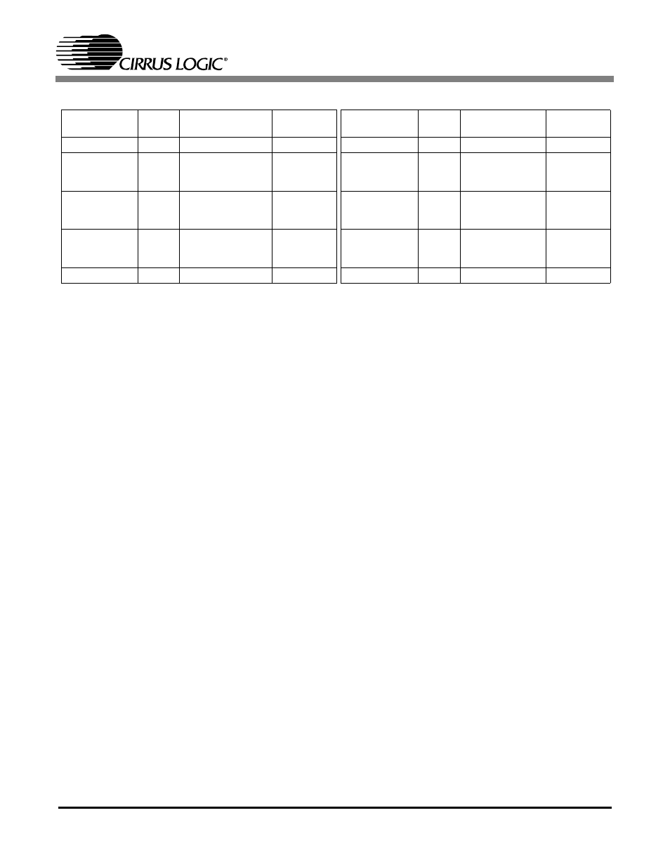
Unipolar Input
Voltage
Offset
Binary
Bipolar Input
Voltage
Two's
Complement
Unipolar Input
Voltage
Offset
Binary
Bipolar Input
Voltage
Two's
Complement
>(VFS-1.5 LSB)
FFFF
>(VFS-1.5 LSB)
7FFF
>(VFS-1.5 LSB) FFFFFF
>(VFS-1.5 LSB)
7FFFFF
VFS-1.5 LSB
FFFF
------
FFFE
VFS-1.5 LSB
7FFF
------
7FFE
VFS-1.5 LSB
FFFFFF
------
FFFFFE
VFS-1.5 LSB
7FFFFF
------
7FFFFE
VFS/2-0.5 LSB
8000
------
7FFF
-0.5 LSB
0000
------
FFFF
VFS/2-0.5 LSB
800000
------
7FFFFF
-0.5 LSB
000000
------
FFFFFF
+0.5 LSB
0001
------
0000
-VFS+0.5 LSB
8001
------
8000
+0.5 LSB
000001
------
000000
-VFS+0.5 LSB
800001
------
800000
<(+0.5 LSB)
0000
<(-VFS+0.5 LSB)
8000
<(+0.5 LSB)
000000
<(-VFS+0.5 LSB)
800000
Table 1: Output Coding for 16-bit CS5531/33 and 24-bit CS5532/34.
CS5531/33 16-Bit Output Coding
CS5532/34 24-Bit Output Coding