An150, How do i use the internal multiplexer in the part, How is the guard drive output pin used – Cirrus Logic AN150 User Manual
Page 11
AN150
AN150REV2
11
Why is the “Common mode + signal on AIN+
or AIN-” specification different for the 1X
gain range?
This difference is due to the fact that there are actu-
ally two different amplifiers inside the converter. In
the 1X gain range, a rail-to-rail, unity-gain amplifi-
er is used. A rail-to-rail amplifier is necessary in the
1X gain range to permit the large input voltage
swings that are expected with this gain range. To
achieve the high level of performance typical of the
CS553x family in the 2X-64X gain ranges, a chop-
per-stabilized, low-drift, multi-path amplifier is
used. The architecture of this amplifier does not
permit rail-to-rail input capability. In the 2X-64X
gain ranges, input signals into the AIN+ and AIN-
inputs must remain higher than (VA- + 0.7 V) and
lower than (VA+ - 1.7 V) for accurate measure-
ments to occur.
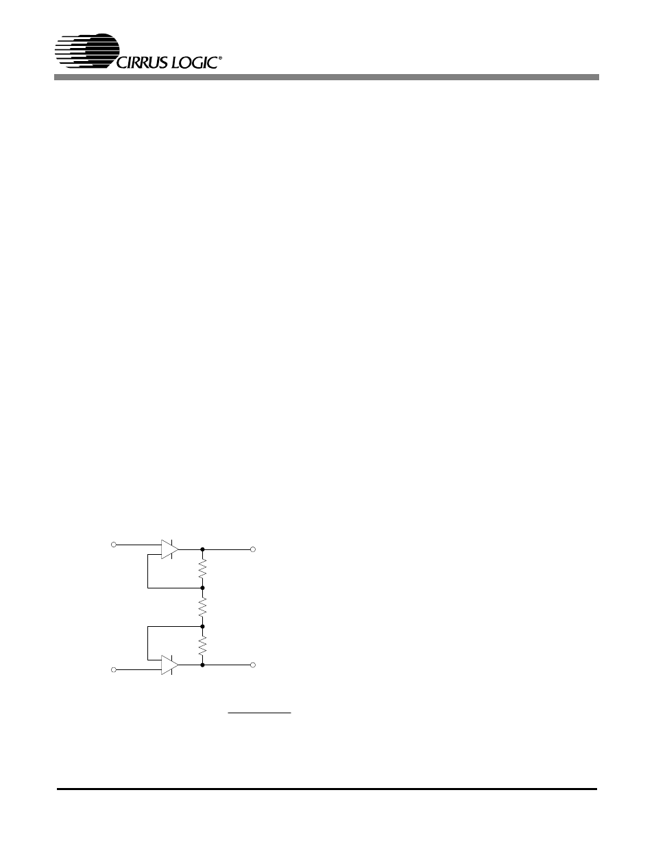
A further consideration is the output of the amplifi-
er. Figure 1 shows a model of the PGIA. In addition
to the common mode requirements on the analog
inputs, the user must ensure that the output of the
amplifier does not become saturated. Using the
equations for V
CM
and V
IN
shown in Figure 1, the
voltages on the output of the amplifier (OUT+ and
OUT-) are equal to V
CM
±
(G
×
V
IN
)/2. The ampli-
fier cannot drive the voltage on the OUT+ or OUT-
pins below (VA- + 0.1 V) or above (VA+ - 0.1 V).
When either OUT+ or OUT- reaches or goes be-
yond these limits, the gain will become (2
×
G)/(G
+ 1). To prevent this from happening, the front-end
circuitry on the ADC should be designed to ensure
that both OUT+ and OUT- remain within these lim-
its at all times.
How do I use the internal multiplexer in the
part?
The different channels of the internal mux can be
selected using the Setups in the Channel Setup
Registers. The most effective way of using the in-
ternal mux is to initiate two or more Setups with
different physical channel values, and then alter-
nate between the Setups as needed while perform-
ing single conversions. Single conversion mode is
recommended when using the internal mux if the
user wants to switch between channels as quickly
as possible. No advantage is gained by using the
continuous conversion mode, since the settling
time for this mode is the same as for the single con-
version mode, and it takes more software overhead
on the microcontroller’s part to start and stop the
conversions. The single conversion mode will en-
sure that each new conversion from the different
mux settings will produce a fully-settled result.
Continuous conversion mode can be useful, how-
ever, if the user wants to convert a single channel
for long periods of time, and only periodically get
a sample from other channels. Data on a single
channel can be collected much faster using this
mode.
How is the guard drive output pin used?
The A0 pin on the CS5531/32/33/34 has a dual
function as both a latch output and an output for the
instrumentation amplifier’s common-mode volt-
age. The setting of the GB bit (bit 26) in the Con-
figuration Register controls which mode this pin is
in. When the GB bit is ‘0’, the A0 pin functions as
2xR
(G-1)xR
(G-1)xR
AIN+
AIN-
OUT+
OUT-
VA-
VA-
VA+
VA+
V
IN
= (AIN+) - (AIN-)
V
CM
=
2
(AIN+) + (AIN-)
Figure 1. Amplifier Model (2X-64X Gain)