6 using multiple adcs synchronously, 7 conversion output coding, Using multiple adcs synchronously – Cirrus Logic CS5530 User Manual
Page 25: Conversion output coding, Figure 12. synchronizing multiple adcs, Table 3. output coding, Cs5530
CS5530
DS742F3
25
2.6 Using Multiple ADCs Synchronously
Some applications require synchronous data out-
puts from multiple ADCs converting different ana-
log channels. Multiple CS5530 devices can be
synchronized in a single system by using the fol-
lowing guidelines:
1) All of the ADCs in the system must be operated
from the same oscillator source.
2) All of the ADCs in the system must share com-
mon SCLK and SDI lines.
3) A software reset must be performed at the same
time for all of the ADCs after system power-up (by
selecting all of the ADCs using their respective CS
pins, and writing the reset sequence to all parts, us-
ing SDI and SCLK).
4) A start conversion command must be sent to all
of the ADCs in the system at the same time. The ±
8 clock cycles of ambiguity for the first conversion
(or for a single conversion) will be the same for all
ADCs, provided that they were all reset at the same
time.
5) Conversions can be obtained by monitoring
SDO on only one ADC, (bring CS high for all but
one part) and reading the data out of each part indi-
vidually, before the next conversion data words are
ready.
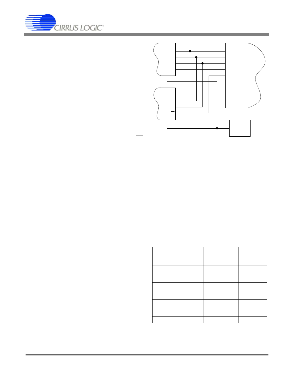
An example of a synchronous system using two
CS5530 devices is shown in Figure 12.
2.7 Conversion Output Coding
The CS5530 outputs 24-bit data conversion words.
To read a conversion word the user must read the
conversion data register. The conversion data reg-
ister is 32 bits long and outputs the conversions
MSB first. The last byte of the conversion data reg-
ister contains an overflow flag bit. The overrange
flag (OF) monitors to determine if a valid conver-
sion was performed.
The CS5530 output data conversions in binary for-
mat when operating in unipolar mode and in two's
complement when operating in bipolar mode. Ta-
ble 3 shows the code mapping for both unipolar and
bipolar modes. VFS in the tables refers to the posi-
tive full-scale voltage range of the converter in the
specified gain range, and -VFS refers to the nega-
tive full-scale voltage range of the converter. The
total differential input range (between AIN+ and
AIN-) is from 0 to VFS in unipolar mode, and from
-VFS to VFS in bipolar mode.
CLOCK
SOURCE
CS5530
CS5530
SDO
SDI
SCLK
CS
OSC2
SDO
SDI
SCLK
CS
OSC2
μC
Figure 12. Synchronizing Multiple ADCs
Table 3. Output Coding
Unipolar Input
Voltage
Offset
Binary
Bipolar Input
Voltage
Two's
Complement
>(VFS-1.5 LSB) FFFFFF >(VFS-1.5 LSB)
7FFFFF
VFS-1.5 LSB
FFFFFF
------
FFFFFE
VFS-1.5 LSB
7FFFFF
------
7FFFFE
VFS/2-0.5 LSB 800000
------
7FFFFF
-0.5 LSB
000000
------
FFFFFF
+0.5 LSB
000001
------
000000
-VFS+0.5 LSB
800001
------
800000
<(+0.5 LSB)
000000 <(-VFS+0.5 LSB)
800000