3 analog section, 1 voltage sensor connection, Figure 2. voltage channel — low-voltage input – Cirrus Logic CDB5490U User Manual
Page 6: Cdb5490u
CDB5490U
6
DS923DB5
1.3
Analog Section
The analog section of the CDB5490U is highly configurable. Onboard signal conditioning options for the
voltage and current channels enable most applications to interface directly to the sensors. The following
two sections define the voltage and current channel configurations.
1.3.1
Voltage Sensor Connection
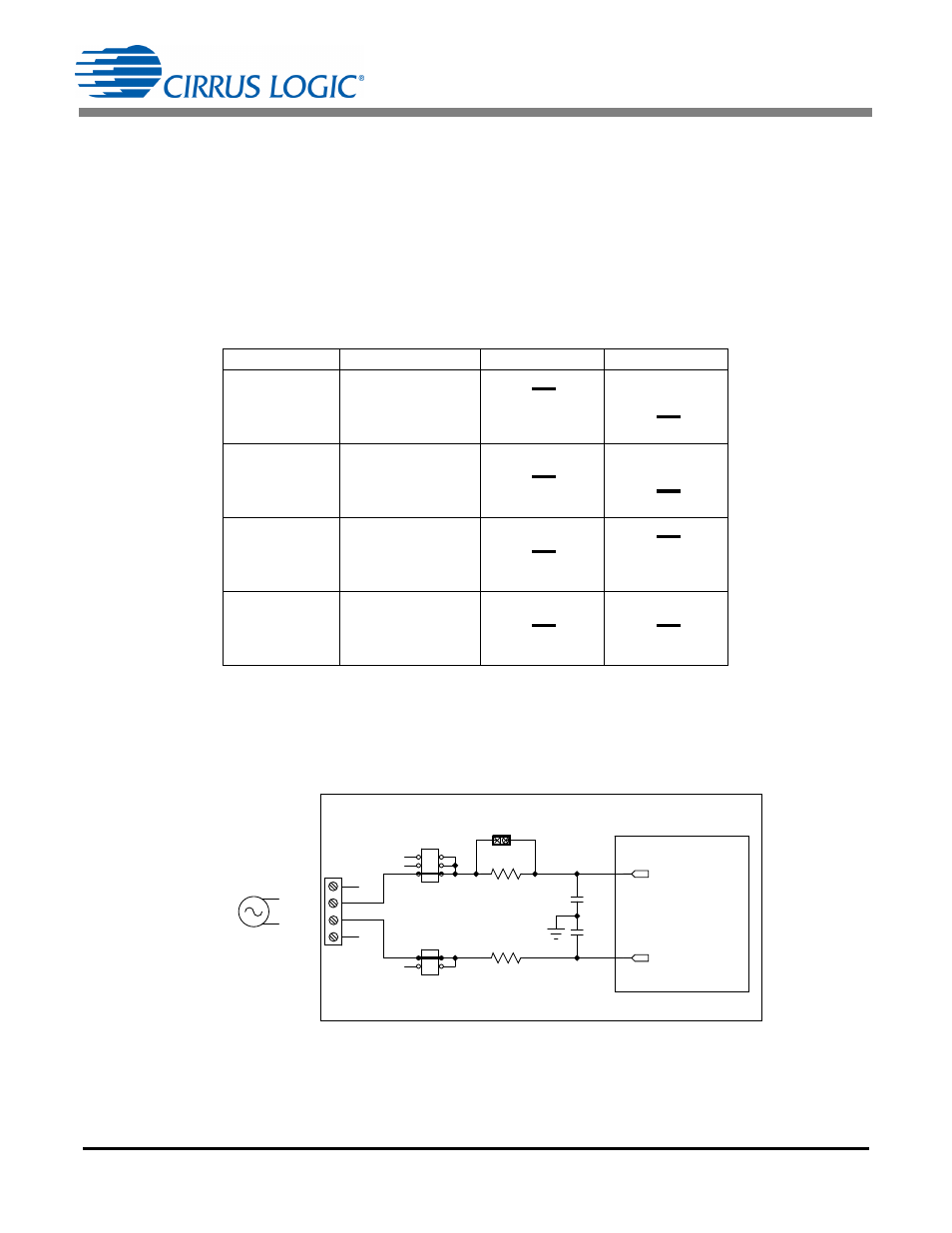
There are three input signal options for the voltage channel input (VIN±): an external low-voltage signal
(via screw terminals or XLR connections), high-voltage line inputs, or GND. Figure 1 illustrates the options
available.
The CDB5490U evaluation board provides screw-type terminals (J3) or XLR connectors (J30) to connect
low-voltage input signals to the voltage channel (see Figure 2). The screw terminals are labeled as
VIN+ / VIN-. An R-C network at the channel input provides a simple, configurable anti-alias filter. By in-
stalling jumpers on J6 to position VIN+ and J11 to position VIN-, the input voltage signal is supplied from
the screw terminals or XLR connections.
The CDB5490U evaluation board provides screw-type terminals (J4) to connect a high-voltage line input.
By installing jumpers on J6 to position LINE and J11 to position GND, the input voltage signal is supplied
from the high-voltage input. Extreme care should be used when connecting high-voltage signals to the
CDB5490U evaluation board (see Figure 3).
Table 1. Voltage Channel Input Signal Selection
INPUT
Description
J11
J6
VIN±
Selects External
Low-voltage Fully
Differential Signal
VIN±
Selects External
Low-voltage Sin-
gle-ended Signal
GND
Selects Grounding
the Input
High-Voltage
Line
Selects External
High-voltage AC
Line Signal
O
VIN-
O O
VIN-
GND
VIN-
(Default)
O
VIN+
O O
VIN+
O O
VIN+
GND
Line
VIN+
(Default)
O
VIN-
O O
VIN-
GND
VIN-
O
VIN+
O O
VIN+
O O
VIN+
GND
Line
VIN+
O
VIN-
O O
VIN-
GND
VIN-
O
VIN+
O O
VIN+
O O
VIN+
GND
Line
VIN+
O
VIN-
O O
VIN-
GND
VIN-
O
VIN+
O O
VIN+
O O
VIN+
GND
Line
VIN+
VIN+
VIN-
250 mVp
CDB5490U
CS5490
J3
J6
J11
C4
0.027UF
C9
0.027UF
R6 1K
R7 1K
J45
VIN+
VIN-
Figure 2. Voltage Channel — Low-voltage Input