Switching characteristics – Cirrus Logic CS5372 User Manual
Page 6
CS5371 CS5372
6
DS255F3
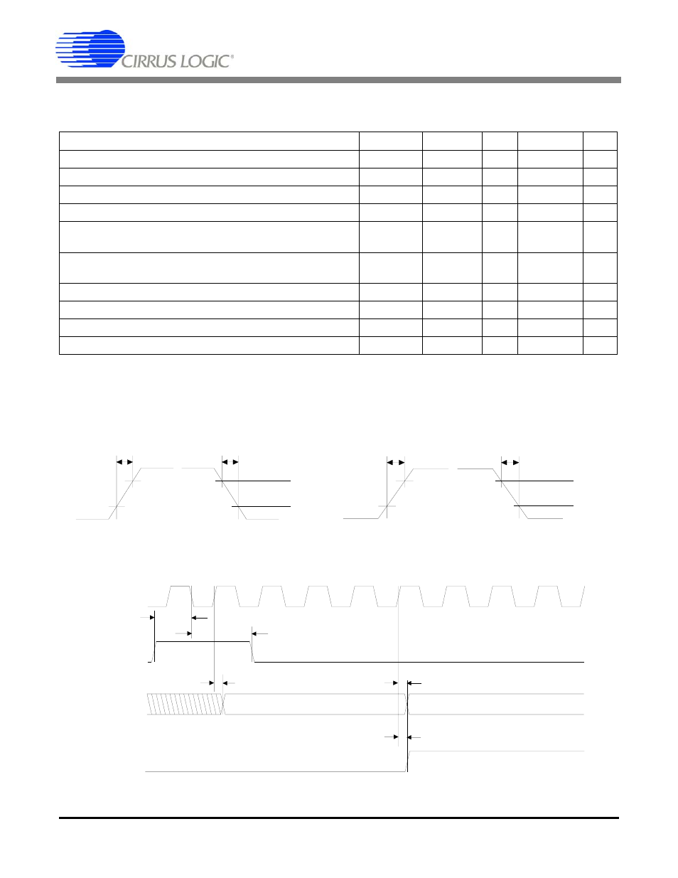
SWITCHING CHARACTERISTICS
Notes:T
A
= -40 C to +85 C; VA+ = +5V or +2.5V ± 5%; VA-
= 0V or -2.5V ± 5%; VD = +5V or +3.3V ± 5%; Digital Inputs: Logic 0 = 0V, Logic 1 = VD; C
L
= 50 pF
Notes: 17. If MCLK is removed, the CS5372 enters a micro power state.
18. Excludes MCLK input, MCLK should be driven with a signal having rise/fall times of 25 ns or faster.
19. MSYNC latched on MCLK falling edge, data output on next MCLK rising edge.
Parameter
Symbol Min Typ
Max
Unit
MCLK Frequency
(Note 17)
f
c
0.1
2.048
2.2
MHz
MCLK Duty Cycle
40
-
60
%
MCLK Jitter (In-band or aliased in-band)
-
-
300
ps
MCLK Jitter (Out-of-band)
-
-
1
ns
Rise Times:
Any Digital Input
(Note 18)
Any Digital Output
t
risein
t
riseout
-
-
-
50
50
100
ns
ns
Fall Times:
Any Digital Input
(Note 18)
Any Digital Output
t
fallin
t
fallout
-
-
-
50
50
100
ns
ns
MSYNC Setup Time to MCLK falling
(Note 19)
t
mss
20
-
-
ns
MSYNC Hold Time after MCLK falling
t
msh
20
-
-
ns
MCLK rising to Valid MFLAG
t
mfh
-
35
65
ns
MCLK rising to Valid MDATA
t
mdv
-
60
90
ns
0.9 * VD
0.1 * VD
t
fallin
t
risein
0.9 * VD
0.1 * VD
t
riseout
t
fallout
Figure 1. Rise and Fall Times
MFLAG
MDATA
t mdv
t mdv
VALID DATA
VALID DATA
MCLK
t mss
MSYNC
t mfh
t msh
Figure 2. CS5372 Interface Timing