Analog characteristics – Cirrus Logic CS5372 User Manual
Page 4
CS5371 CS5372
4
DS255F3
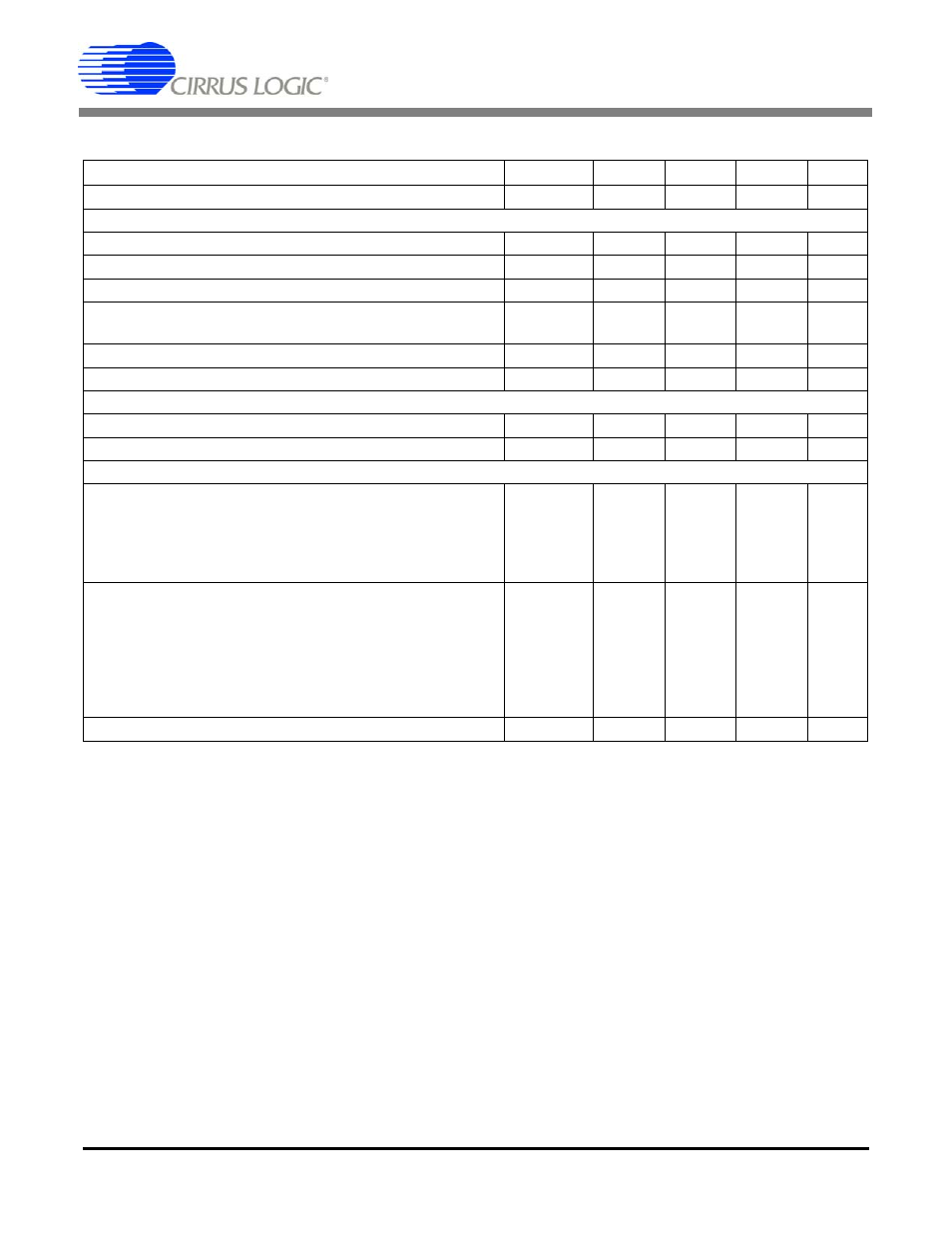
ANALOG CHARACTERISTICS
(Continued)
Notes: 7. The upper bandwidth limit is determined by the digital filter. A simple single pole anti-alias filter with a -
3 dB frequency at (MCLK / 256) should be placed in front of each channel.
8. The input voltage range is for the configuration depicted in Figure 3, the System Connection Diagram,
and applies to signal frequencies from DC to the stop-band frequency selected in the digital filter.
9. Per channel. All outputs unloaded. All digital inputs forced to VD or GND respectively.
10. In Low Power Mode LPWR = 1, the Master Clock MCLK is reduced to 1.024 MHz. This reduces the
oversampled signal bandwidth by a factor of 2.
11. Tested with a 50 Hz 100 mVpp sine wave applied separately to each supply.
Parameter
Symbol Min Typ
Max
Unit
Specified Temperature Range
T
A
-40
-
+85
C
Input Characteristics
Input Signal Frequencies
(Note 7)
BW
DC
-
1720
Hz
Input Voltage Range
(Note 8)
VIN
-
-
5
V
p-p
Input Over-range Voltage Tolerance
(Note 8)
I
OVR
5
-
-
%F.S.
Input Signal plus Common Mode
(VA-)
+ 0.7V
-
(VA+)
- 1.7V
V
Common Mode Rejection Ratio
CMRR
-
90
-
dB
Channel Crosstalk (CS5372 only)
CXT
-
-120
-
dB
Voltage Reference Input
VREF
(VREF+) - (VREF-)
-
2.5
-
V
VREF Current
-
-
120
µA
Power Supplies
DC Power Supply Currents
(Note 9 and 10)
LPWR = 0; MCLK = 2.048 MHz
Analog
Digital
LPWR = 1; MCLK = 1.024 MHz
Analog
Digital
VA
VD
VA
VD
-
-
-
-
5.0
0.2
3.0
0.2
7.0
0.3
4.5
0.3
mA
mA
mA
mA
Power Down Modes
CS5371
PWDN = 1
PWDN = 1, MCLK = 0
CS5372
PWDN1 or PWDN2 = 1
PWDN1 = PWDN2 = 1
PWDN1 = PWDN2 = 1, MCLK = 0
P
D
-
-
-
-
-
1
10
25
1
10
-
-
-
-
-
mW
µW
mW
mW
µW
Power Supply Rejection
(Note 11)
PSRR
-
90
-
dB