Pin description - cs5372 – Cirrus Logic CS5372 User Manual
Page 18
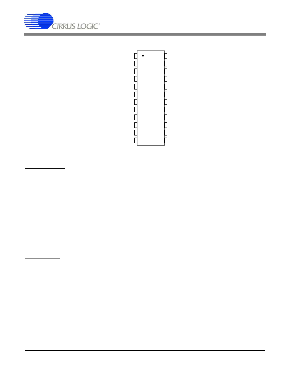
CS5371 CS5372
18
DS255F3
11. PIN DESCRIPTION - CS5372
Power Supplies
VA+
_
Positive Analog Power Supply, pin 8
Positive supply voltage.
VA-
_
Negative Analog Power Supply, pin 7
Negative supply voltage.
VD
_
Positive Digital Power Supply, pin 18
Positive supply voltage.
DGND
_
Digital Ground, pin 17
Analog Inputs
INR1+, INR2+
_
Channel 1 & 2 Rough Non-Inverting Inputs, pin 1, 12
Rough non-inverting analog inputs. The rough inputs settle non-linear currents to improve
linearity on the fine inputs and reduce harmonic distortion.
INR1-, INR2-
_
Channel 1 & 2 Rough Inverting Inputs, pin 4, 9
Rough inverting analog inputs. The rough inputs settle non-linear currents to improve linearity
on the fine inputs and reduce harmonic distortion.
INF1+, INF2+
_
Channel 1 & 2 Fine Non-Inverting Input, pin 2, 11
Fine non-inverting analog inputs.
1
2
3
4
5
6
7
8
17
18
19
20
21
22
23
24
9
10
11
12
13
14
15
16
Ch. 1 Rough Non-Inverting Input
INR1+
Ch. 1 Fine Non-Inverting Input
INF1+
Ch. 1 Fine Inverting Input
INF1-
Ch. 1 Rough Inverting Input
INR1-
Positive Voltage Reference Input
VREF+
Negative Voltage Reference Input
VREF-
Negative Analog Power Supply
VA-
Positive Analog Power Supply
VA+
Ch. 2 Rough Inverting Input
INR2-
Ch. 2 Fine Inverting Input
INF2-
Ch. 2 Fine Non-Inverting Input
INF2+
Ch. 2 Rough Non-Inverting Input
INR2+
PWDN1
Ch. 1 Power-down Enable
LPWR
Low Power Mode Select
MFLAG1
Ch. 1 Modulator Flag Output
MDATA1
Ch. 1 Modulator Data Output
MSYNC
Modulator Sync Input
MCLK
Modulator Clock Input
VD
Positive Digital Power Supply
DGND
Digital Ground
MDATA2
Ch. 2 Modulator Data Output
MFLAG2
Ch. 2 Modulator Flag Output
OFST
Offset Mode Select
PWDN2
Ch. 2 Power-down Enable