Cirrus Logic CS5372 User Manual
Modulators, Features & description, Description
Copyright
© Cirrus Logic, Inc. 2005
(All Rights Reserved)
CS5371
CS5372
Low-power, High-performance
∆Σ
Modulators
Features
& Description
z
Fourth-order
∆Σ Architecture
z
Clock-jitter-tolerant Architecture
z
Input Voltage: 5 V
pp
Fully Differential
z
High Dynamic Range
127 dB SNR @ 215 Hz BW (2 ms Output)
124 dB SNR @ 430 Hz BW (1 ms Output)
z
Low Total Harmonic Distortion
-118 dB THD Typical, -112 dB THD Maximum
z
Low Power Consumption
Normal Mode: 25 mW per Channel
Low-power Mode: 15 mW per Channel
z
Small Footprint, 24-pin SSOP Package
z
Single- or Multi-channel System Support
1-channel System: CS5371
2-channel System: CS5372
3-channel System: CS5371 + CS5372
4-channel System: CS5372 + CS5372
z
Single or Dual Power Supply Configurations
VA+ = +5 V; VA- = 0 V; VD = +3.3 V to +5 V
VA+ = +2.5 V;VA- = -2.5 V;VD = +3.3 V
Description
The CS5371 and CS5372 are one- and two-channel,
high dynamic range, fourth-order
∆Σ modulators intend-
ed for geophysical and sonar applications. Used in
combination with the CS5376A or CS5378 digital filters,
a unique high-resolution A/D measurement system
results.
The CS5371 and CS5372 have high dynamic range
(127 dB @ 215 Hz bandwidth) and low total harmonic
distortion (typically -118 dB THD), with very low power
consumption per channel. In normal mode
(LPWR=0, MCLK=2.048MHz), power consumption is
25 mW per channel, and in low-power mode
(LPWR=1, MCLK=1.024MHz), power consumption is
15 mW per channel. Each modulator can be indepen-
dently powered down to 1 mW per channel, and by
halting the input clock, they will enter a micropower state
using only 10 µW per channel.
The modulators generate an oversampled serial bit
stream at 512 kbits per second when operated from a
clock frequency of 2.048 MHz. They are available in a
small 24-pin SSOP package, providing exceptional per-
formance in a very small footprint.
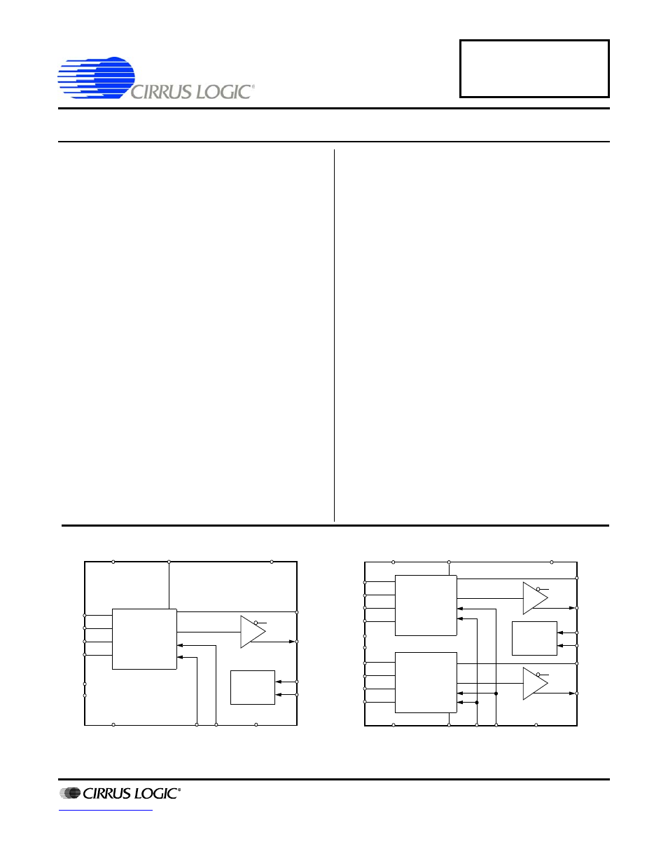
ORDERING INFORMATION
INF1+
VA+
4
TH
ORDER
INR1+
INR1-
VREF+
VREF-
MDATA2
MSYNC
MCLK
PWDN1
VD
∆−Σ MODULATOR
INF1-
PWDN2
INF2+
4
TH
ORDER
INR2+
INR2-
∆−Σ MODULATOR
INF2-
OFST LPWR
DGND
MFLAG2
CLOCK
GENERATOR
MDATA1
MFLAG1
VA-
INF+
VA+
4
TH
ORDER
INR+
INR-
VREF+
VREF-
MSYNC
MCLK
PWDN
VD
∆−Σ MODULATOR
INF-
OFST LPWR
DGND
CLOCK
GENERATOR
MDATA
MFLAG
VA-
CS5371
CS5372
OCT ‘05
DS255F3
Document Outline
- Features & Description
- 1. Characteristics & Specifications
- 2. General Description.
- 4. Signal Inputs
- 5. Input Offset
- 6. Voltage Reference Inputs
- 7. Digital Filter Interface
- 8. Power Modes
- 9. Power Supply
- 10. Pin Description - CS5371
- 11. Pin Description - CS5372
- 12. Package Dimensions
- 13. Ordering Information
- 14. Environmental, Manufacturing, & Handling Information
- 15. Revision History