General description, 1 system design, 1 master clock – Cirrus Logic CS5331A User Manual
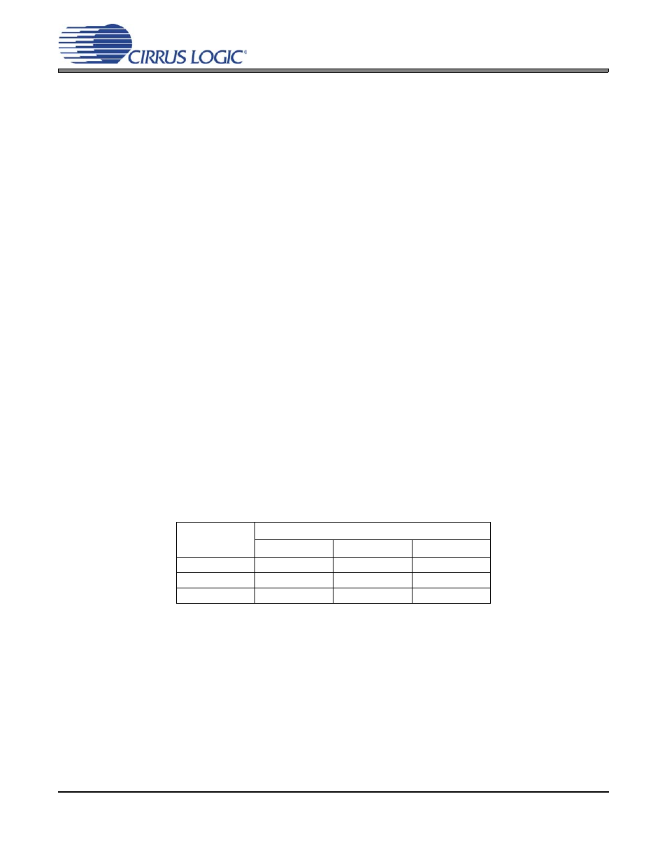
Page 9: 2 serial data interface, Table 1. common clock frequencies, 3 master mode, Common clock frequencies
DS138F6
9
CS5330A/31A
3. GENERAL DESCRIPTION
The CS5330A and CS5331A are 18-bit, 2-channel Analog-to-Digital Converters designed for digital audio applica-
tions. Each device uses two one-bit delta-sigma modulators which simultaneously sample the analog input signals
at 128 times the output sample rate (Fs). The resulting serial bit streams are digitally filtered, yielding pairs of 18-bit
values. This technique yields nearly ideal conversion performance independent of input frequency and amplitude.
The converters do not require difficult-to-design or expensive anti-alias filters and do not require external sample-
and-hold amplifiers or a voltage reference.
The CS5330A and CS5331A differ only in the output serial data format. These formats are discussed in the following
sections and shown in
An on-chip voltage reference provides for a single-ended input signal range of 4.0 Vpp. Output data is available in
serial form, coded as 2’s complement 18-bit numbers. Typical power consumption is 150 mW which can be further
reduced to 0.5 mW using the Power-Down mode.
For more information on delta-sigma modulation, see the references at the end of this data sheet.
3.1
System Design
Very few external components are required to support the ADC. Normal power supply decoupling compo-
nents and a resistor and capacitor on each input for anti-aliasing are all that are required, as shown in
3.1.1
Master Clock
The master clock (MCLK) runs the digital filter and is used to generate the delta-sigma modulator sam-
pling clock.
shows some common master clock frequencies. The output sample rate is equal to
the frequency of the Left / Right Clock (LRCK). The serial nature of the output data results in the left and
right data words being read at different times. However, the words within an LRCK cycle represent simul-
taneously sampled analog inputs. The serial clock (SCLK) shifts the digitized audio data from the internal
data registers via the SDATA pin.
3.1.2
Serial Data Interface
The CS5330A and CS5331A can be operated in either Master mode, where SCLK and LRCK are outputs,
or SLAVE mode, where SCLK and LRCK are inputs.
3.1.3
Master Mode
In Master mode, SCLK and LRCK are outputs which are internally derived from MCLK. The CS5330A/31A
will divide MCLK by 4 to generate a SCLK which is 64
Fs and by 256 to generate LRCK. The CS5330A
and CS5331A can be placed in the Master mode with a 47-k
pull-down resistor on the SDATA pin as
LRCK
(kHz)
MCLK (MHz)
256x
384x
512x
32
8.1920
12.2880
16.3840
44
11.2896
16.9344
22.5792
48
12.2880
18.4320
24.5760
Table 1. Common Clock Frequencies