4 slave mode, 5 cs5330a, 6 cs5331a – Cirrus Logic CS5331A User Manual
Page 10: Figure 2. data output timing-cs5330a, 4 slave mode 3.1.5 cs5330a 3.1.6 cs5331a, Figure 2, Data output timing-cs5330a, Data output timing - cs5331a (i, Figures 2
10
DS138F6
CS5330A/31A
3.1.4
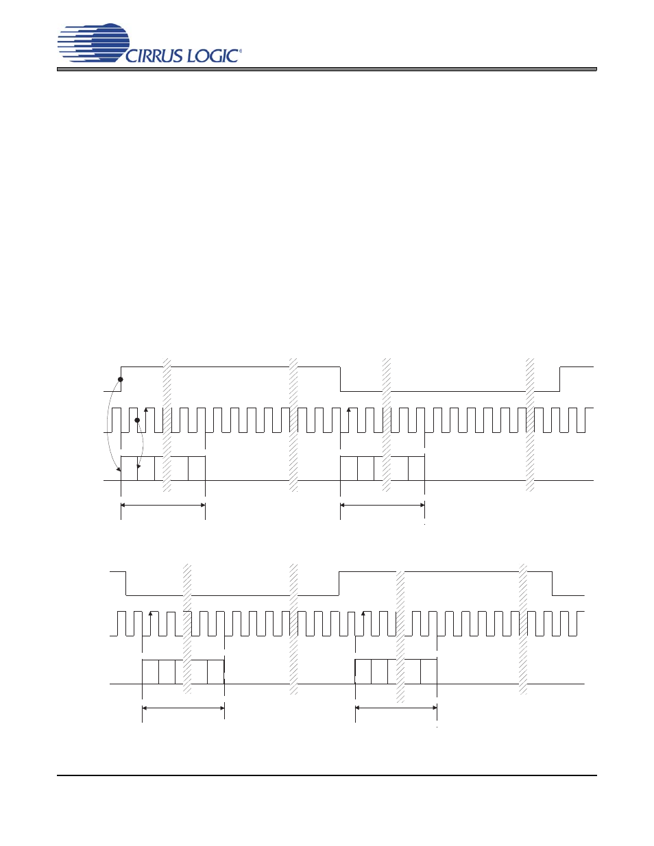
Slave Mode
LRCK and SCLK become inputs in SLAVE mode. LRCK must be externally derived from MCLK and be
equal to Fs. The frequency of SCLK should be equal to 64x
LRCK, though other frequencies are possible.
MCLK frequencies of 256x, 384x, and 512x
Fs are supported. The ratio of the applied MCLK to LRCK is
automatically detected during power-up and internal dividers are set to generate the appropriate internal
clocks.
3.1.5
CS5330A
The CS5330A data output format is shown in
. Notice that the MSB is clocked by the transition of
LRCK and the remaining seventeen data bits are clocked by the falling edge of SCLK. The data bits are
valid during the rising edge of SCLK.
3.1.6
CS5331A
The CS5331A data output format is shown in
. Notice the one SCLK period delay between the
LRCK transitions and the MSB of the data. The falling edges of SCLK cause the ADC to output the eigh-
teen data bits. The data bits are valid during the rising edge of SCLK. LRCK is also inverted compared to
the CS5330A interface. The CS5331A interface is compatible with I
2
S.
0
1
2
18
19
20 21 22
31 0 1 2
18
19
20 21 22
23
31 0 1
SCLK
LRCK
Left Audio Data
Right Audio Data
17
16
1
0
17
16
1
0
SDATA
17 17
30
Figure 2. Data Output Timing-CS5330A
0
1
2
18
19
20 21
22 31
0
1
2
18
19
20 21
22
23
31 0 1
SCLK
LRCK
Left Audio Data
Right Audio Data
17
16
1
0
17
16
1
0
SDATA
3
3
30
Figure 3. Data Output Timing - CS5331A (I²S Compatible)