10 grounding and power supply decoupling, Figure 4, Upon initial – Cirrus Logic CS5331A User Manual
Page 12: Own in
12
DS138F6
CS5330A/31A
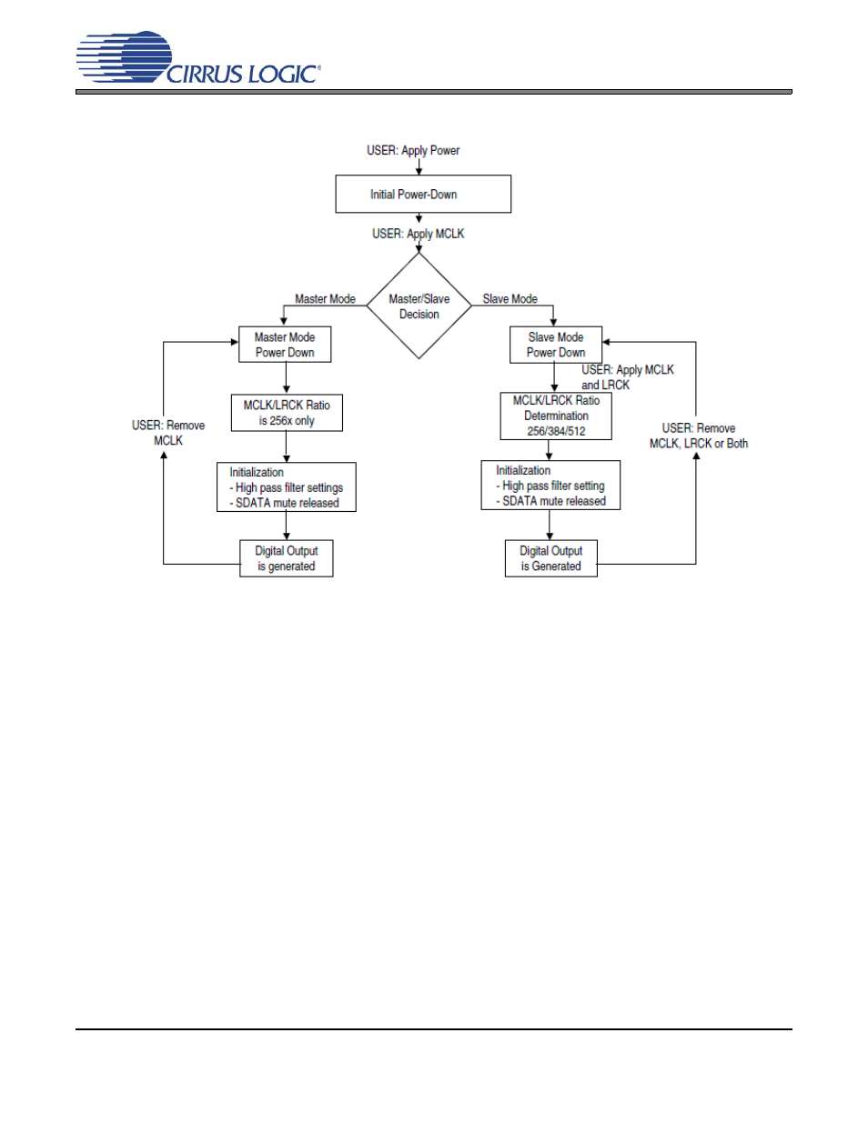
The CS5330A and CS5331A have a Power-Down mode wherein typical consumption drops to 0.5 mW.
This is initiated when a loss of clock is detected on either the LRCK or MCLK pins in Slave Mode, or the
MCLK pin in Master Mode. The initialization sequence will begin when MCLK (and LRCK for slave mode)
are restored. In slave mode power-down, the CS5330A and CS5331A will adapt to changes in
MCLK/LRCK frequency ratio during the initialization sequence. It is recommended that clocks not be ap-
plied to the device prior to power supply settling. A reset circuit may be implemented by gating the MCLK
signal.
3.1.10
Grounding and Power Supply Decoupling
As with any high resolution converter, the ADC requires careful attention to power supply and grounding
arrangements if its potential performance is to be realized. Figure 1 shows the recommended power ar-
rangements with VA+ connected to a clean +5-V supply. Decoupling capacitors should be as near to the
ADC as possible, with the low value ceramic capacitor being the nearest. To minimize digital noise, con-
nect the ADC digital outputs only to CMOS inputs. The printed circuit board layout should have separate
analog and digital regions and ground planes. An evaluation board, CDB5330A or CDB5331A, is avail-
able which demonstrates the optimum layout and power supply arrangements, as well as allowing fast
evaluation of the CS5330A and CS5331A.
Figure 4. CS5330A/31A Initialization and Power-Down Sequence