Pin descriptions – Cirrus Logic CS5331A User Manual
Page 3
DS138F6
3
CS5330A/31A
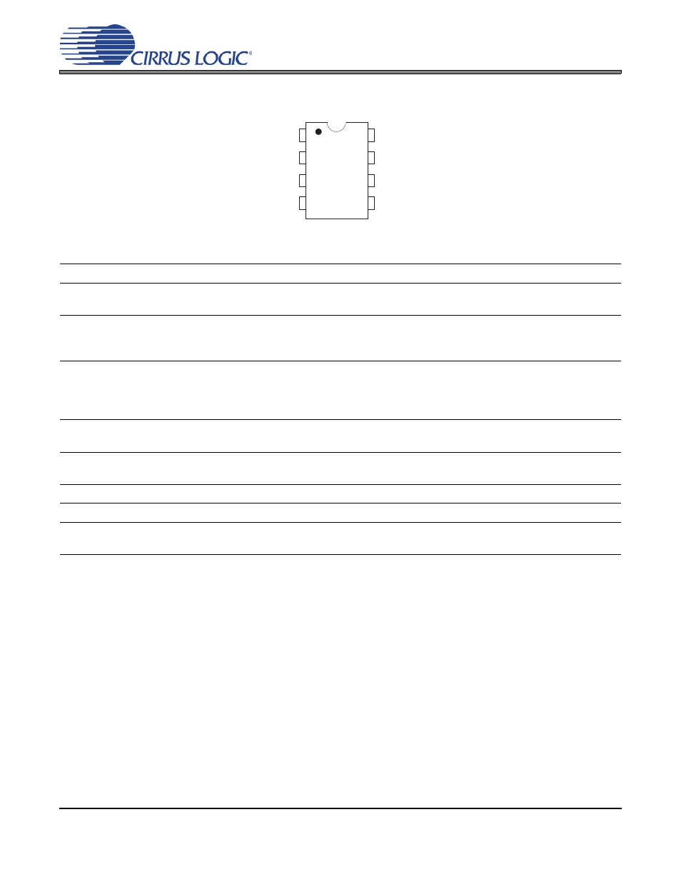
1. PIN DESCRIPTIONS
Pin Name
#
Pin Description
SDATA
1
Audio Serial Data Output (Output) - Two’s complement MSB-first serial data is output on this
pin. A 47 k
resistor on this pin will place the CS5330A/31A into Master Mode.
SCLK
2
Serial Data Clock (Input/Output) - SCLK is an input clock at any frequency from 32x to 64x the
output word rate. SCLK can also be an output clock at 64x if in the Master Mode. Data is
clocked out on the falling edge of SCLK.
LRCK
3
Left/Right Clock (Input/Output) - LRCK selects the left or right channel for output on SDATA.
The LRCK frequency must be at the output sample rate. LRCK is an output clock if in Master
Mode. Although the outputs of each channel are transmitted at different times, the two words in
an LRCK cycle represent simultaneously sampled analog inputs.
MCLK
4
Master Clock Input (Input) - Source for the delta-sigma modulator sampling and digital filter
clock. Sample rates and digital filter characteristics scale to the MCLK frequency.
AINR
5
Analog Right Channel Input (Input) - Analog input for the right channel. Typically 4 Vpp for a
full-scale input signal.
AGND
6
Analog Ground (Input) - Analog ground reference.
VA+
7
Positive Analog Power (Input) - Positive analog supply (Nominally +5 V).
AINL
8
Analog Left Channel Input (Input) - Analog input for the left channel. Typically 4 Vpp for a full-
scale input signal.
7
2
6
3
5
4
8
1
SERIAL DATA OUTPUT
SERIAL DATA CLOCK
LEFT/RIGHT CLOCK
MASTER CLOCK
LEFT ANALOG INPUT
ANALOG POWER
ANALOG GROUND
RIGHT ANALOG INPUT
SDATA
SCLK
LRCK
MCLK
AINL
VA+
AGND
AINR