Cirrus Logic CS43L22 User Manual
Cs43l22, Low power, stereo dac w/headphone & speaker amps, Confidential draft 3/4/10
Copyright
Cirrus Logic, Inc. 2010
(All Rights Reserved)
MARCH '10
DS792F2
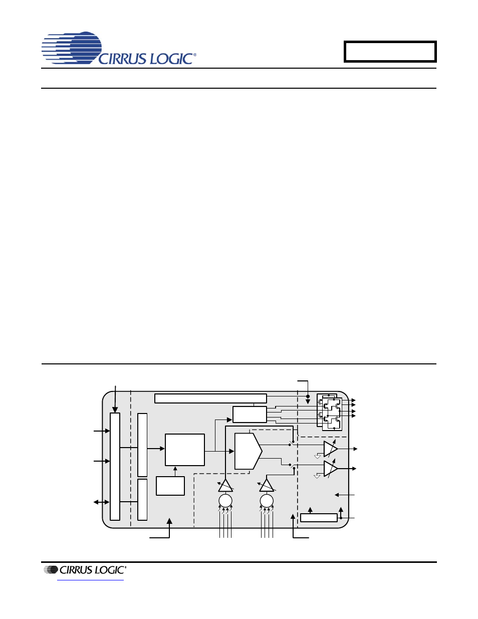
Low Power, Stereo DAC w/Headphone & Speaker Amps
FEATURES
98 dB Dynamic Range (A-wtd)
88 dB THD+N
Headphone Amplifier - GND Centered
–
No DC-Blocking Capacitors Required
–
Integrated Negative Voltage Regulator
–
2 x 23 mW into Stereo 16
Ω @ 1.8 V
–
2 x 44 mW into Stereo 16
Ω @ 2.5V
Stereo Analog Input Passthrough Architecture
–
Analog Input Mixing
–
Analog Passthrough with Volume Control
Digital Signal Processing Engine
–
Bass & Treble Tone Control, De-Emphasis
–
PCM Input w/Independent Vol Control
–
Master Digital Volume Control and Limiter
–
Soft-Ramp & Zero-Cross Transitions
Programmable Peak-Detect and Limiter
Beep Generator w/Full Tone Control
–
Tone Selections Across Two Octaves
–
Separate Volume Control
–
Programmable On and Off Time Intervals
–
Continuous, Periodic, One-Shot Beep
Selections
Class D Stereo/Mono Speaker Amplifier
No External Filter Required
High Stereo Output Power at 10% THD+N
–
2 x 1.00 W into 8
Ω @ 5.0 V
–
2 x 550 mW into 8
Ω @ 3.7 V
–
2 x 230 mW into 8
Ω @ 2.5 V
High Mono Output Power at 10% THD+N
–
1 x 1.90 W into 4
Ω @ 5.0 V
–
1 x 1.00 W into 4
Ω @ 3.7 V
–
1 x 350 mW into 4
Ω @ 2.5 V
Direct Battery Powered Operation
–
Battery Level Monitoring & Compensation
81% Efficiency at 800 mW
Phase-Aligned PWM Output Reduces Idle
Channel Current
Spread Spectrum Modulation
Low Quiescent Current
+1.60 V to +5.25 V
Battery
+1.65 V to +2.63 V
Digital Supply
Pulse-Width
Modulator
Battery Level Monitoring & Compensation
Multi-bit
ΔΣ DAC
Le
ve
l S
h
if
te
r
+1.65 V to +3.47 V
Interface Supply
Control Po
rt
S
e
ri
al A
u
d
io
Port
Beep
Generator
Digital Volume,
Mono Mix,
Limiter, Bass,
Treble Adjust
Left
Inputs
Σ
4
3
2
1
Summing
Amplifiers
Left HP/Line
Output
Ground-Centered
Amps
Right HP/Line
Output
+1.65 V to +2.63 V
Headphone Supply
Speaker/HP
Switch
Charge Pump
+VHP
-VHP
+1.65 V to +2.63 V
Analog Supply
Stereo/Mono
Full-Bridge
Speaker
Outputs
Class D Amps
+
-
+
-
I²C
Control
Reset
Serial
Audio
Input
Right
Inputs
Σ
4
3
2
1
CS43L22
Confidential Draft
3/4/10
Document Outline
- Table of Contents
- List of Figures
- 1. Pin Descriptions
- 2. Typical Connection Diagram
- 3. Characteristic and Specifications
- 4. Applications
- 5. Control Port Operation
- 6. Register Quick Reference
- 7. Register Description
- 7.1 Chip I.D. and Revision Register (Address 01h) (Read Only)
- 7.2 Power Control 1 (Address 02h)
- 7.3 Power Control 2 (Address 04h)
- 7.4 Clocking Control (Address 05h)
- 7.5 Interface Control 1 (Address 06h)
- 7.6 Interface Control 2 (Address 07h)
- 7.7 Passthrough x Select: PassA (Address 08h), PassB (Address 09h)
- 7.8 Analog ZC and SR Settings (Address 0Ah)
- 7.9 Passthrough Gang Control (Address 0Ch)
- 7.10 Playback Control 1 (Address 0Dh)
- 7.11 Miscellaneous Controls (Address 0Eh)
- 7.12 Playback Control 2 (Address 0Fh)
- 7.13 Passthrough x Volume: PASSAVOL (Address 14h) & PASSBVOL (Address 15h)
- 7.14 PCMx Volume: PCMA (Address 1Ah) & PCMB (Address 1Bh)
- 7.15 Beep Frequency & On Time (Address 1Ch)
- 7.16 Beep Volume & Off Time (Address 1Dh)
- 7.17 Beep & Tone Configuration (Address 1Eh)
- 7.18 Tone Control (Address 1Fh)
- 7.19 Master Volume Control: MSTA (Address 20h) & MSTB (Address 21h)
- 7.20 Headphone Volume Control: HPA (Address 22h) & HPB (Address 23h)
- 7.21 Speaker Volume Control: SPKA (Address 24h) & SPKB (Address 25h)
- 7.22 PCM Channel Swap (Address 26h)
- 7.23 Limiter Control 1, Min/Max Thresholds (Address 27h)
- 7.24 Limiter Control 2, Release Rate (Address 28h)
- 7.25 Limiter Attack Rate (Address 29h)
- 7.26 Status (Address 2Eh) (Read Only)
- 7.27 Battery Compensation (Address 2Fh)
- 7.28 VP Battery Level (Address 30h) (Read Only)
- 7.29 Speaker Status (Address 31h) (Read Only)
- 7.30 Charge Pump Frequency (Address 34h)
- 8. Analog Performance Plots
- 9. Example System Clock Frequencies
- 10. PCB Layout Considerations
- 11. Digital Filter Plots
- 12. Parameter Definitions
- 13. Package Dimensions
- 14. Ordering Information
- 15. References
- 16. Revision History