Figure 13. dsd phase modulation mode diagram, Cs4398 – Cirrus Logic CS4398 User Manual
Page 24
24
DS568F1
CS4398
4.7.6
Direct Stream Digital (DSD) Mode (Control Port Mode)
In Control Port mode, the FM bits (Reg. 02h) are used to configure the device for DSD mode. The DIF
bits (Reg 02h) then control the expected DSD rate and MCLK ratio.
The DSD_SRC bit (Reg. 02h) selects the input pins for DSD clocks and data. During DSD operation, the
PCM-related pins should either be tied low or remain active with clocks. When the DSD related pins are
not being used, they should either be tied low or remain active with clocks.
The DIR_DSD bit (Reg 07h) selects between two proprietary methods for DSD-to-analog conversion. The
first method uses a decimation-free DSD processing technique that allows for features such as matched
PCM level output, DSD volume control, and 50 kHz on-chip filter. The second method sends the DSD data
directly to the on-chip switched-capacitor filter for conversion (without the above mentioned features).
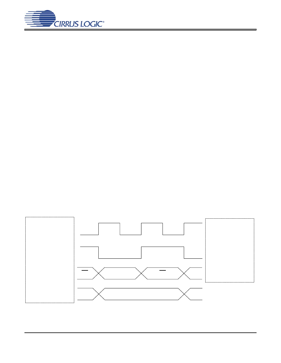
The DSD_PM_EN bit (Reg. 09h) selects Phase Modulation (data plus data inverted) as the style of data
input. In this mode, the DSD_PM_mode bit selects whether a 128Fs or 64x clock is used for phase mod-
ulated 64x data (see Figure 13). Use of phase modulation mode may not directly effect the performance
of the CS4398, but may lower the sensitivity to board-level routing of the DSD data signals.
The CS4398 can detect errors in the DSD data that do not comply to the SACD specification. The
STATIC_DSD and INVALID_DSD bits (Reg. 09h) allow the CS4398 to alter the incoming invalid DSD da-
ta. Depending on the error, the data may either be attenuated or replaced with a muted DSD signal (the
MUTEC pins would set according to the DAMUTE bit (Reg. 04h)).
More information for any of these register bits can be found in the Register Description section.
The DSD input structure and analog outputs are designed to handle a nominal 0 dB-SACD (50% modu-
lation index) at full rated performance. Signals of +3 dB-SACD may be applied for brief periods of time;
however, performance at these levels is not guaranteed. If sustained +3 dB-SACD levels are required,
the digital volume control should be set to -3.0 dB. This same volume control register affects PCM output
levels. There is no need to change the volume control setting between PCM and DSD in order to have the
0 dB output levels match (both 0 dBFS and 0 dB-SACD will output at -3 dB in this case).
Figure 13. DSD Phase Modulation Mode Diagram
BCKA
(128Fs)
BCKD
(64Fs)
DSD_SCLK
DSD_A,
DSD_B
D1
D1
D1
D0
D2
D2
D0
DSD_SCLK
DSD_A,
DSD_B
BCKA
(64Fs)
DSD_SCLK
DSD Phase
M odulation M ode
DSD Norm al M ode