Cirrus Logic CS4398 User Manual
Cs4398, Features, Supports stand-alone or i²c/spi
Copyright
© Cirrus Logic, Inc. 2005
(All Rights Reserved)
120 dB, 192 kHz Multi-Bit DAC with Volume Control
Features
Advanced Multi-bit Delta-Sigma Architecture
– 120 dB Dynamic Range
– -107 dB THD+N
– Low Clock Jitter Sensitivity
– Differential Analog Outputs
PCM input
– 102 dB of Stopband Attenuation
– Supports Sample Rates up to 192 kHz
– Accepts up to 24 bit Audio Data
– Supports All Industry Standard Audio
Interface Formats
– Selectable Digital Filter Response
– Volume Control with 1/2 dB Step Size and
Soft Ramp
– Flexible Channel Routing and Mixing
– Selectable De-Emphasis
Supports Stand-Alone or I²C/SPI
™
Configuration
Embedded Level Translators
– 1.8 V to 5 V Serial Audio Input
– 1.8 V to 5 V Control Data Input
Direct Stream Digital (DSD)
– Dedicated DSD Input Pins
– On-Chip 50 kHz Filter to Meet Scarlet Book
SACD Recommendations
– Matched PCM and DSD Analog Output
Levels
– Non-Decimating Volume Control with
1/2 dB Step Size and Soft Ramp
– DSD Mute Detection
– Supports Phase-Modulated Inputs
– Optional Direct DSD Path to On-Chip
Switched Capacitor Filter
Control Output for External Muting
– Independent Left and Right Mute Controls
– Supports Auto Detection of Mute Output
Polarity
Typical Applications
– DVD Players
– SACD Players
– A/V Receivers
– Professional Audio Products
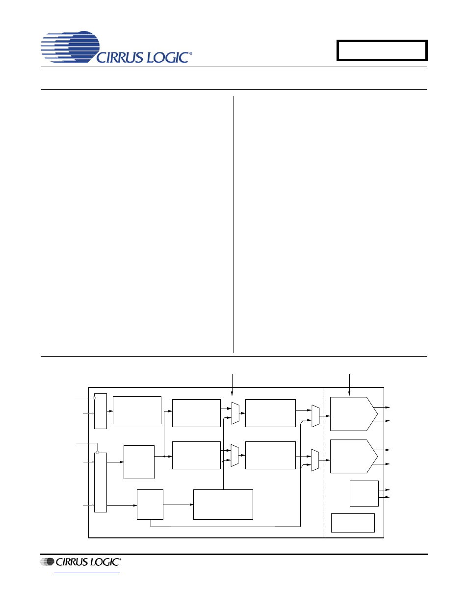
PCM
Serial
Interface
Multibit
∆Σ
Modulator
Interpolation
Filter with
Volume Control
Internal Voltage
Reference
External
Mute
Control
Switched
Capacitor
DAC and
Filter
DSD
Interface
PCM Input
Left and Right
Mute Controls
Right
Differential
Output
Left
Differential
Output
DSD Input
DSD Processor
1.8 V to 5V
1.8 V to 5 V
-Volume control
-50kHz filter
Switched
Capacitor
DAC and
Filter
MU
X
Direct DSD
Lev
el
T
rans
lat
or
Le
v
e
l
Tr
a
n
s
la
to
r
Hardware or I
2
C/SPI
Control Data
MUX
Multibit
∆Σ
Modulator
Interpolation
Filter with
Volume Control
MUX
MUX
3.3 V to 5 V
5 V
Register/Hardware
Configuration
JULY '05
DS568F1
CS4398
Document Outline
- 1. Pinout Drawing
- 2. Characteristics and Specifications
- Specified Operating Characteristics
- Absolute Maximum Ratings
- Analog Characteristics
- Combined Interpolation & On-chip Analog Filter Response
- DSD Combined Digital & On-chip Analog Filter Response
- Switching Characteristics
- Switching characteristics - DSD
- Switching Characteristics - Control Port - I2C format
- Switching Characteristics - Control Port - SPI™ Format
- DC Electrical Characteristics
- Digital Interface Specifications
- 3. Typical Connection Diagram
- 4. Applications
- 4.1 Grounding and Power Supply Decoupling
- 4.2 Analog Output and Filtering
- 4.3 The MUTEC Outputs
- 4.4 Oversampling Modes
- 4.5 Master and Serial Clock Ratios
- 4.6 Stand-alone Mode Settings
- 4.7 Control Port Mode
- 4.7.1 Recommended Power-up Sequence (Control Port Mode)
- 4.7.2 Sample Rate Range/Oversampling Mode (Control Port Mode)
- 4.7.3 Serial Audio Interface Formats (Control Port Mode)
- 4.7.4 MUTEC Pins (Control Port Mode)
- 4.7.5 Interpolation Filter (Control Port Mode)
- 4.7.6 Direct Stream Digital (DSD) Mode (Control Port Mode)
- 5. Control Port Interface
- 5.1 Memory Address Pointer (MAP)
- 5.2 Enabling the Control Port
- 5.3 Format Selection
- 5.4 I2C Format
- 5.5 SPI Format
- 7.1 Chip ID - Register 01h
- 7.2 Mode Control 1 - Register 02h
- 7.3 Volume Mixing and Inversion Control - Register 03h
- 7.4 Mute Control - Register 04h
- 7.5 Channel A Volume Control - Register 05h
- 7.6 Channel B Volume Control - Register 06h
- 7.7 Ramp and Filter Control - Register 07h
- 7.8 Misc. Control - Register 08h
- 7.9 Misc. Control - Register 09h
- 8. Parameter Definitions
- 9. References
- 10. Package Dimensions
- 11. Appendix