Applications, 1 recommended power-up sequence for hardware mode, 3 analog output and filtering – Cirrus Logic CS4391A User Manual
Page 33: Figure 15. cs4391a output filter, Cs4391a, 1) hold, High
CS4391A
DS600PP3
33
7. APPLICATIONS
7.1
Recommended Power-up
Sequence for Hardware Mode
1) Hold
RST
low until the power supplies, master,
and left/right clocks are stable.
2) Bring
RST
high.
7.2
Recommended Power-up
Sequence and Access to Control
Port Mode
1) Hold
RST
low until the power supply, master,
and left/right clocks are stable. In this state, the
control port is reset to its default settings and
CMOUT will remain low.
2) Bring
RST
high. The device will remain in a
low power state with CMOUT low and the con-
trol port is accessible.
3) Write 30h to register 5 within 10 ms cycles fol-
lowing the release of RST.
4) The desired register settings can be loaded
while keeping the PDN bit set to 1.
5) Set the PDN bit to 0 which will initiate the pow-
er-up sequence which requires approximately
10 µS.
7.3
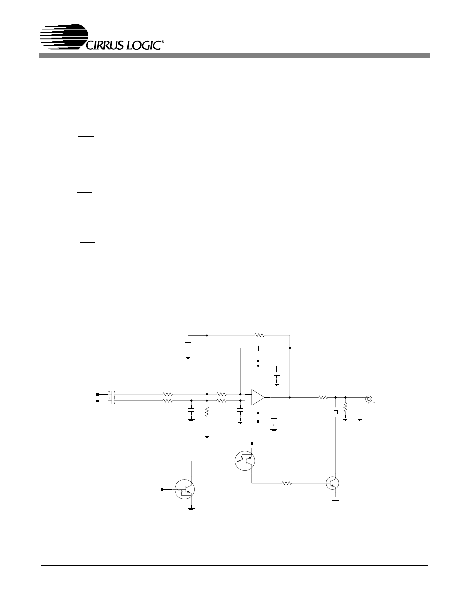
Analog Output and Filtering
The application note “Design Notes for a 2-Pole
Filter with Differential Input” discusses the second-
order Butterworth filter and differential to single-
ended converter which was implemented on the
CS4391A evaluation board, CDB4391A. The
CS4391A filter, as seen in Figure 14, is a linear
phase design and does not include phase or ampli-
tude compensation for an external filter. Therefore,
the DAC system phase and amplitude response will
be dependent on the external analog circuitry.
AMUTEC
AOUTA+
GND
C43
10UF
GND
GND
GND
1.18K
R17
NC
4
3
2
1
CON_RCA_RA
J3
2
3
1
2SC2878
Q1
2K
R25
3
1
2
Q3
MMUN2111LT1
12
HDR8
HDR1X2
AOUTA
VA+3/+5
R20
560
3
1
2
Q4
MMUN2211LT1
R24
5.62K
R5
47K
R28
5.62K
1.18K
R18
5.62K
R15
5.62K
R26
C49
.1UF
V-
V+
+
-
4
8
1
2
3
U11
MC33078D
C48
.1UF
GND
GND
GND
GND
GND
GND
C42
10UF
COG
2700PF
C7
COG
560PF
C6
COG
C5
560PF
COG
2700PF
C14
VCC
VEE
AOUTA-
Figure 15. CS4391A Output Filter