Pin description - dsd mode, Cs4391a – Cirrus Logic CS4391A User Manual
Page 26

CS4391A
26
DS600PP3
6.
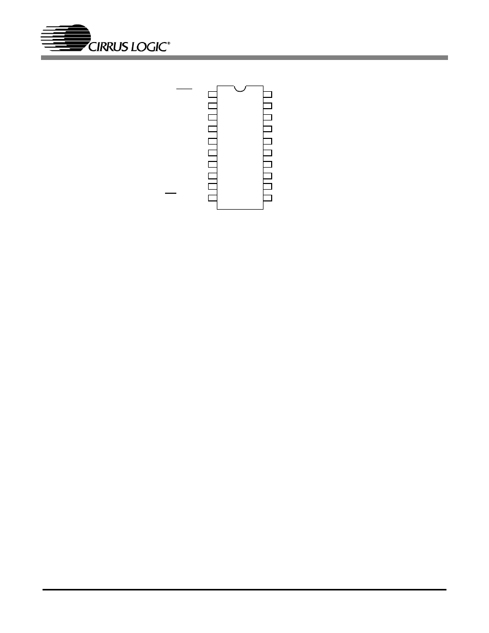
PIN DESCRIPTION - DSD MODE
DSD Audio Data - DSD_A and DSD_B
Pins 3 and 4, Inputs
Function:
Direct Stream Digital audio data is clocked into DSD_A and DSD_B via the DSD serial clock.
DSD Mode - DSD_Mode
Pin 5, Input
Function:
This pin must be set to a logic ‘1’ and M0-M2 must be properly set to access the DSD Mode in Hardware
Mode. Refer to Table 2.
In Control Port Mode, this pin must be set to a logic ‘1’ and the Control Registers must be properly set to
access the DSD Mode. Refer to register descriptions.
Master Clock - MCLK
Pin 6, Input
Function:
The master clock frequency must be either 4x, 6x, 8x or 12x the DSD data rate for 64x oversampled DSD
data or 2x, 3x, 4x or 6x the DSD data rate for 128x oversampled DSD data.
DSD Serial Clock - DSD_SCLK
Pin 7, Input
Function:
Clocks the individual bits of the DSD audio data into the DSD_A and DSD_B pins.
Reset
RST
AMUTEC
Refer to PCM Mode
Logic Voltage
VL
AOUTA-
Refer to PCM Mode
Channel A Data
DSD_A
AOUTA+
Refer to PCM Mode
Channel B Data
DSD_B
VA
Refer to PCM Mode
DSD Mode Select
DSD_MODE
AGND
Refer to PCM Mode
Master Clock
MCLK
AOUTB+
Refer to PCM Mode
DSD Serial Clock
DSD_SCLK
AOUTB-
Refer to PCM Mode
Refer to PCM Mode (SCL/CCLK) M2
BMUTEC
Refer to PCM Mode
Refer to PCM Mode (SDA/CDIN) M1
CMOUT
Refer to PCM Mode
Refer to PCM Mode
(AD0/CS) M0
FILT+
Refer to PCM Mode
1
2
3
4
20
19
18
17
5
6
7
8
16
15
14
13
9
10
12
11
