Pin description - pcm data mode, Cs4391a – Cirrus Logic CS4391A User Manual
Page 22
CS4391A
22
DS600PP3
5.
PIN DESCRIPTION - PCM DATA MODE
Reset - RST
Pin 1, Input
Function:
Hardware Mode: The device enters a low power mode and the internal state machine is reset to the de-
fault setting when low. When high, the device becomes operational.
Control Port Mode: The device enters a low power mode and all internal registers are reset to the default
settings, including the control port, when low. When high, the control port becomes operational and the
PDN bit must be cleared before normal operation will occur. The control port can not be accessed when
reset is low. The Control Port Enable Bit must also be enabled after a device reset.
RST is required to remain low until the power supplies and clocks are applied and stable.
Interface Power - VL
Pin 2, Input
Function:
Digital interface power supply. The voltage on this pin determines the logic level high threshold for the
digital inputs.
Serial Audio Data - SDATA
Pin 3, Input
Function:
Two's complement MSB-first serial data is input on this pin. The data is clocked into SDATA via the serial
clock and the channel is determined by the Left/Right clock. The required relationship between the
Left/Right clock, serial clock and serial data is defined by the Mode Control Byte in Control Port Mode or
the Mode Pins in Hardware Mode. The options are detailed in Figures 7-24.
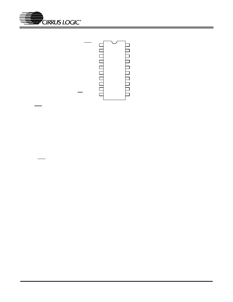
Reset
RST
AMUTEC
Channel A Mute Control
Logic Voltage
VL
AOUTA-
Differential Output
Serial Data
SDATA
AOUTA+
Differential Output
Serial Clock
SCLK
VA
Analog Power
Left/Right Clock
LRCK
AGND
Analog Ground
Master Clock
MCLK
AOUTB+
Differential Output
See Description
M3
AOUTB-
Differential Output
See Description (SCL/CCLK) M2
BMUTEC
Channel B Mute Control
See Description (SDA/CDIN) M1
CMOUT
Common Mode Voltage
See Description
(AD0/CS) M0
FILT+
Positive Voltage Reference
1
2
3
4
20
19
18
17
5
6
7
8
16
15
14
13
9
10
12
11