Pin descriptions – Cirrus Logic CS4354 User Manual
Page 4
4
DS895F2
CS4354
1. PIN DESCRIPTIONS
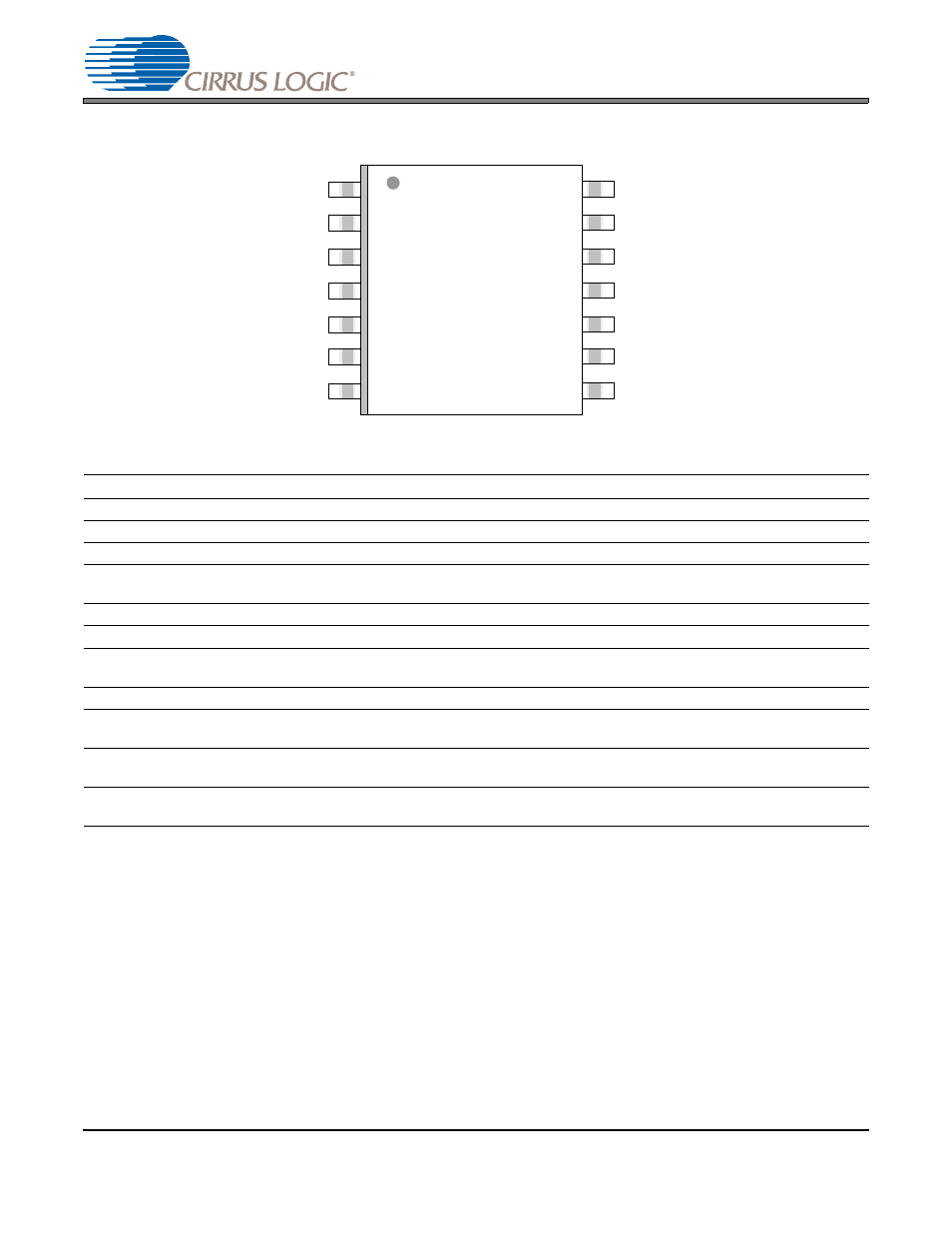
Pin Name Pin #
Pin Description
VL
1
Serial Audio Interface Power (Input) - Positive power for the serial audio interface.
SDIN
2
Serial Audio Data Input (Input) - Input for two’s complement serial audio data.
MCLK
3
Master Clock (Input) - Clock source for the delta-sigma modulator and digital filters.
LRCK
4
Left / Right Clock (Input) - Determines which channel, Left or Right, is currently active on the serial
audio data line.
SCLK/DEM
5
Serial Clock (Input) - Serial clock for the serial audio interface.
FILT+
7
Positive Voltage Reference (Output) - Positive reference voltage for the internal sampling circuits.
AOUTA
AOUTB
8
9
Analog Outputs (Output) - The full-scale analog line output level is specified in the Analog Characteris-
tics table.
GND
6, 10 Ground (Input) - Ground reference. See
for layout considerations.
VA
11
Analog, Charge Pump, and Regulator Power (Input) - Positive power supply for the analog, inverting
charge pump, and regulator for the digital core logic sections.
FLYP
FLYN
12
13
Inverting Charge Pump Cap Positive/Negative Nodes (Output) - Positive and Negative nodes for the
inverting charge pump’s flying capacitor.
-VFILT
14
Inverting Charge Pump Filter Connection (Output) - Power supply from the inverting charge pump that
provides the negative rail for the output amplifiers.
VL
-VFILT
SDIN
FLYN
MCLK
FLYP
LRCK
VA
SCLK/DEM
GND
GND
AOUTB
FILT+
AOUTA
1
2
3
4
5
6
7
9
10
11
12
13
14
8