Dc electrical characteristics, 1 digital i/o pin characteristics, Table 2. digital i/o pin characteristics – Cirrus Logic CS4354 User Manual
Page 11: Cs4354 dc electrical characteristics
DS895F2
11
CS4354
DC ELECTRICAL CHARACTERISTICS
Test conditions (unless otherwise specified): VA = 5 V, VL = 3.3 V; GND = 0 V; SDIN = 0; all voltages with respect
to ground.
Notes: 15. Power supply current increases with increasing sample rate and increasing MCLK frequency. Typical
values are based on Fs = 48 kHz and MCLK = 12.288 MHz. Maximum values are based on highest
sample rate and highest MCLK frequency; see
“Switching Specifications - Serial Audio Interface” on
. Variance between speed modes is small.
16. During normal operation, SDIN = 997 Hz sine wave at 0 dBFS with load resistance R
L
= 3
k
.
17. Power-down is defined as all clock and data lines held static low. All digital inputs have a weak pull-
down (approximately 50 k
) which is only present during power on reset. Opposing this pull-down will
increase the power-down current.
18. Valid with the recommended capacitor values as shown in the
“Typical Connection Diagram” on
2.1
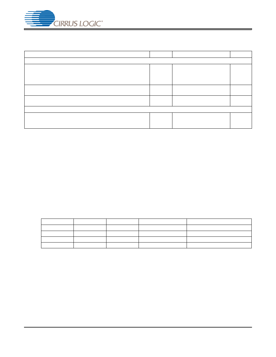
Digital I/O Pin Characteristics
Input and output levels and associated typical power supply voltage are shown in
. Logic levels
should not exceed the corresponding power supply voltage.
Table 2. Digital I/O Pin Characteristics
Parameters
Symbol
Min
Typ
Max
Units
Power Supplies
Power supply current
Normal operation
Power-down
I
VA
I
VL
I
VA
I
VL
-
-
-
-
10
0.1
0.5
1
13
0.2
-
-
mA
mA
mA
A
Power dissipation (all supplies)
Normal Operation
Power-Down
-
-
50
2.5
65
-
mW
mW
Power supply rejection ratio
(1
kHz)
(60 Hz)
PSRR
-
-
60
60
-
-
dB
dB
DC Output Voltages
Pin voltage
FILT+ to GND
FLYP to FLYN
GND to -VFILT
-
-
-
3.5
4.9
4.7
-
-
-
V
V
V
Pin Name
Power Supply
I/O
Driver
Receiver
MCLK
VL
Input
-
1.8 V - 5 V
LRCK
VL
Input
-
1.8 V - 5 V
SCLK
VL
Input
-
1.8 V - 5 V
SDIN
VL
Input
-
1.8 V - 5 V