3 de-emphasis, 4 initialization and power-down, 5 output transient control – Cirrus Logic CS4348 User Manual
Page 15: 1 power-up, 2 power-down, 1 power-up 4.5.2 power-down, Figure 10.de-emphasis curve (fs = 44.1khz)
15
CS4344/5/8
4.3
De-Emphasis
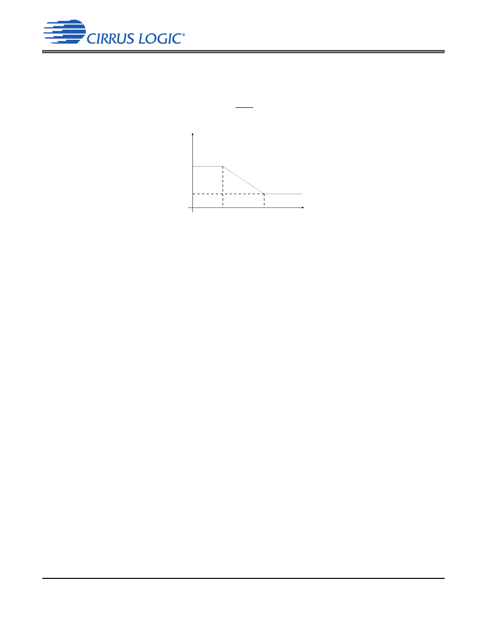
The CS4344 family includes on-chip digital deemphasis.
shows the deemphasis curve for Fs
equal to 44.1 kHz. The frequency response of the deemphasis curve will scale proportionally with changes
in sample rate, Fs.
The deemphasis filter is active (inactive) if the DEM/SCLK pin is low (high) for 5 consecutive falling edges
of LRCK. This function is available only in the internal serial clock mode
.
Figure 10. De-Emphasis Curve (Fs = 44.1kHz)
4.4
Initialization and Power-Down
The Initialization and Power-down sequence flow chart is shown in
. The CS4344 family enters the
Power-Down State upon initial power-up. The interpolation filters and delta-sigma modulators are reset, and the
internal voltage reference, multi-bit digital-to-analog converters and switched-capacitor low-pass filters are pow-
ered down. The device will remain in the Power-down mode until MCLK and LRCK are present. Once MCLK and
LRCK are detected, MCLK occurrences are counted over one LRCK period to determine the MCLK/LRCK fre-
quency ratio. Power is then applied to the internal voltage reference. Finally, power is applied to the D/A converters
and switched-capacitor filters, and the analog outputs will ramp to the quiescent voltage, VQ.
4.5
Output Transient Control
The CS4344 family uses Popguard
®
technology to minimize the effects of output transients during power-
up and power-down. This technique eliminates the audio transients commonly produced by single-ended
single-supply converters when it is implemented with external DC-blocking capacitors connected in series
with the audio outputs. To make best use of this feature, it is necessary to understand its operation.
4.5.1
Power-Up
When the device is initially powered-up, the audio outputs, AOUTL and AOUTR, are clamped to VQ which
is initially low. After MCLK is applied, the outputs begin to ramp with VQ towards the nominal quiescent
voltage. This ramp takes approximately 250 ms with a 3.3 µF cap connected to VQ (420 ms with a 10 µF
connected to VQ) to complete. The gradual voltage ramping allows time for the external DC-blocking ca-
pacitors to charge to VQ, effectively blocking the quiescent DC voltage. Once valid LRCK and SDIN are
supplied (and SCLK if used) approximately 2000 sample periods later audio output begins.
4.5.2
Power-Down
To prevent audio transients at power-down, the DC-blocking capacitors must fully discharge before turn-
ing off the power. To accomplish this, MCLK should be stopped for a period of about 250 ms for a 3.3 µF
cap connected to VQ (420 ms for a 10 µF cap connected to VQ) before removing power. During this time
voltage on VQ and the audio outputs discharge gradually to GND. If power is removed before this time
period has passed a transient will occur when the VA supply drops below that of VQ. There is no minimum
time for a power cycle; power may be re-applied at any time.
Gain
dB
-10dB
0dB
Frequency
T2 = 15 µs
T1=50 µs
F1
F2
3.183 kHz
10.61 kHz