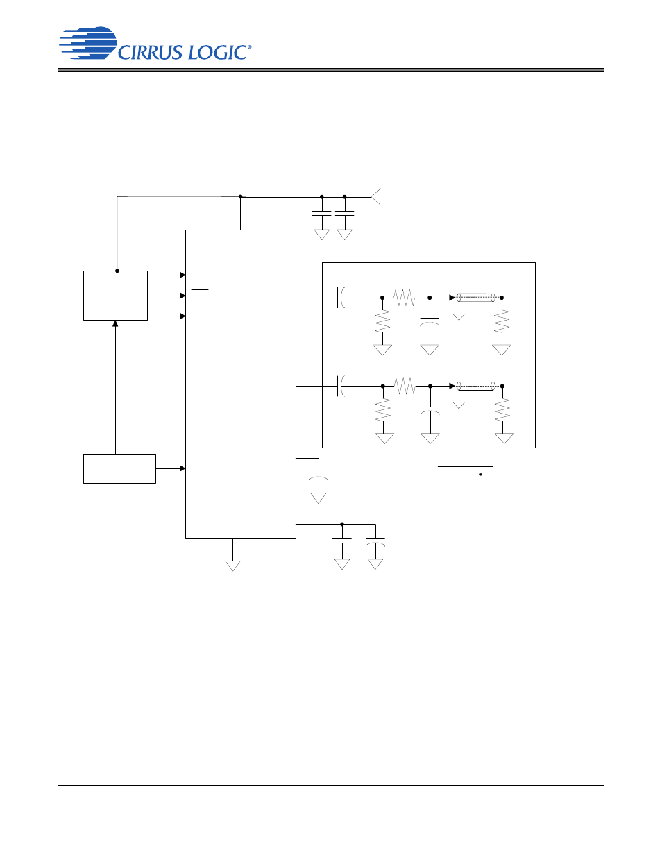
Typical connection diagram, Figure 6.typical connection diagram, Section 3 – Cirrus Logic CS4348 User Manual
Page 11
11
CS4344/5/8
3. TYPICAL CONNECTION DIAGRAM
Figure 6. Typical Connection Diagram
DEM/SCLK
8
Audio
Data
Processor
External Clock
MCLK
AGND
AOUTR
CS4344
CS4345
CS4348
SDIN
LRCK
VA
AOUTL
3
1
2
4
9
0.1 µF
+
1 µF
7
Left Audio
Output
10
Right Audio
Output
+3.3 V to +5 V
3.3 µF
10 k
C
470
+
R
+ 470
C =
4Fs(R
470)
R
ext
3.3 µF
10 k
C
470
+
R
ext
ext
ext
+
0.1 µF
10
µF
+
*3.3
µF
6
VQ
FILT+
5
Note*
Note* = This circuitry is intended for applications where the
CS4344/5/8 connects directly to an unbalanced output of
the design. For internal routing applications please see the
DAC analog output characteristics for loading limitations.
For best 20 kHz response
µF
*10
*Popguard ramp can be adjusted by
selecting this capacitor value to be
3.3 µF to give 250 ms ramp time
or 10 µF to give a 420 ms ramp
time.
or