3 configuration options, 1 s/pdif or psia in to analog out, Configuration options – Cirrus Logic CDB42L55 User Manual
Page 8: Figure 2.s/pdif or psia in to analog out, Software
8
DS773DB1
CDB42L55
3 CONFIGURATION OPTIONS
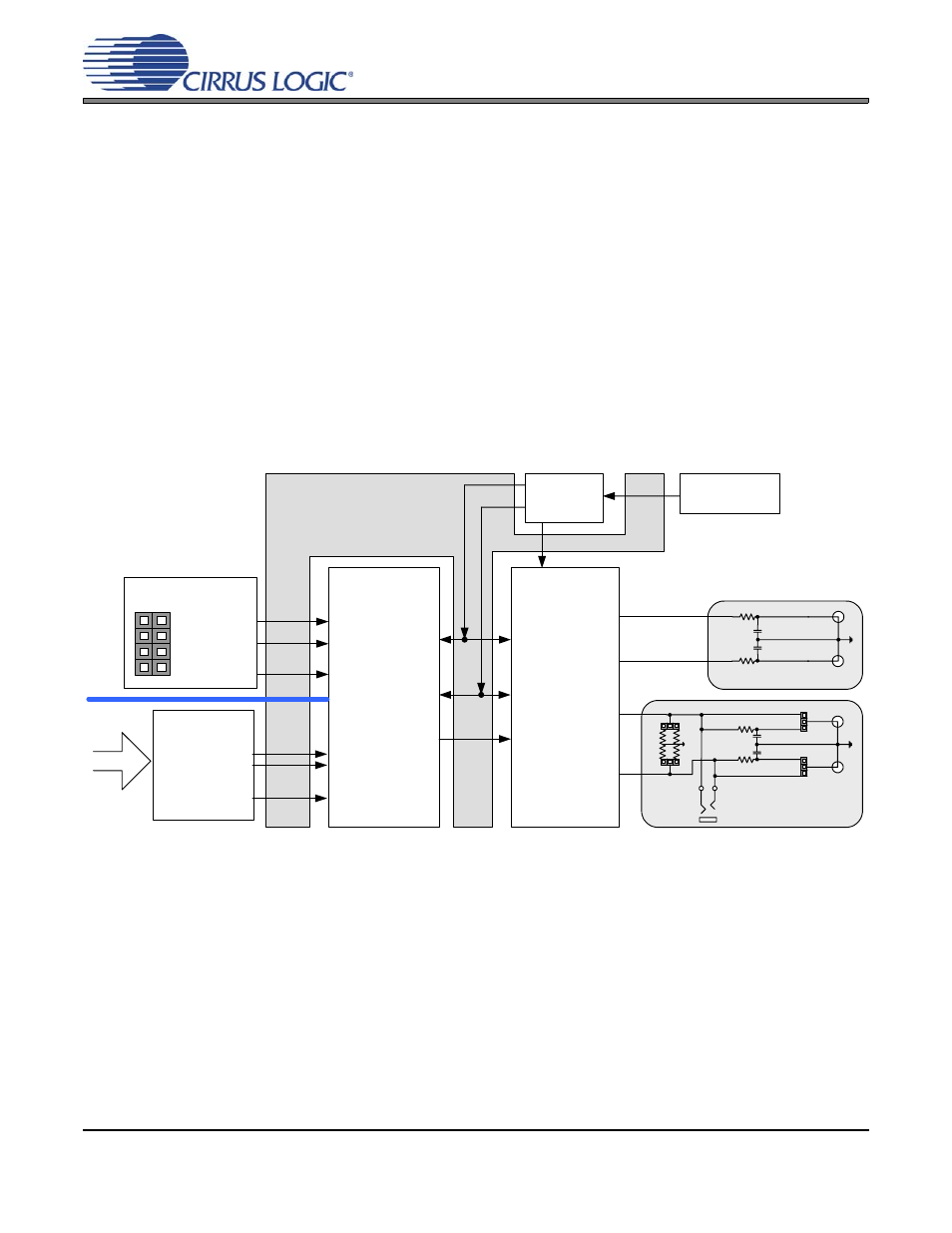
This section highlights two common configurations for the CDB42L55. It provides a basic understanding of how the
various components on the board work together.
3.1
S/PDIF or PSIA In to Analog Out
The CS42L55 analog back-end performance can be tested by selecting the “SPDIF In to Analog Out --
Analog In to S/PDIF Out” or “PSIA In to Analog Out -- Analog In to PSIA Out” quick setup file provided
with the software package. Note: The Control Port Compensation script for the associated VA supply
must also be selected. The script configures the digital clock and data signal routing on the board as shown
in
. The quick setup scripts provided in the software assume that a 24.000 MHz on-board oscillator
is populated in Y1.
A S/PDIF input must be provided as the S/PDIF Tx (CS8406) uses the RMCK signal from the S/PDIF Rx
(CS8416) for synchronization in this configuration.
Figure 2. S/PDIF or PSIA In to Analog Out
PSIA Tx (J78)
TX.SCLK
TX.LRCK
TX.SDOUT
Tx SRC
(CS8421)
PLL
24 MHz
(on-board osc.)
An on-board PLL generates all supported sample and
bit clock rates from an on-board 24 MHz oscillator.
Out
Out
S/PDIF Rx
(CS8416)
RX.LRCK
RX.SCLK
RX.SDOUT
S/PDIF
IN
LRCK
CS42L55
SCLK
DAC.SDIN
32
32
16
16
J2
J3
J4
J12
HP
Connection
HP
Channel
J21
B
A
Line
Channel
B
A
LINEOUTB
LINEOUTA
HPOUTB
HPOUTA
FPGA
(Master)
(Slave)
(Slave)
MCLK