Cirrus Logic CDB42L55 User Manual
Cdb42l55, Evaluation board for cs42l55, Features
Copyright
© Cirrus Logic, Inc. 2008
(All Rights Reserved)
Evaluation Board for CS42L55
Features
Line-level Analog Inputs
–
4 RCA Input Jacks
Line-Level & HP Analog Output
–
Stereo Headphone Out Jack
–
RCA Audio Jacks for Headphone and Line
Outputs
S/PDIF Interface
–
CS8416 Digital Audio Receiver
–
CS8406 Digital Audio Transmitter
I/O Stake Headers and SMA Connectors
–
External I²C
™
Control Port Accessibility
–
External DSP Serial Audio I/O Accessibility
–
Direct DSP Serial Audio I/O accessibility
with CS42L55 through SMA connectors
Multiple Power Supply options via USB, Battery
or External Power Supplies
1.65 V to 3.3 V Logic Interface
FlexGUI S/W Control - Windows
®
Compatible
–
Pre-defined & User-configurable Scripts
Description
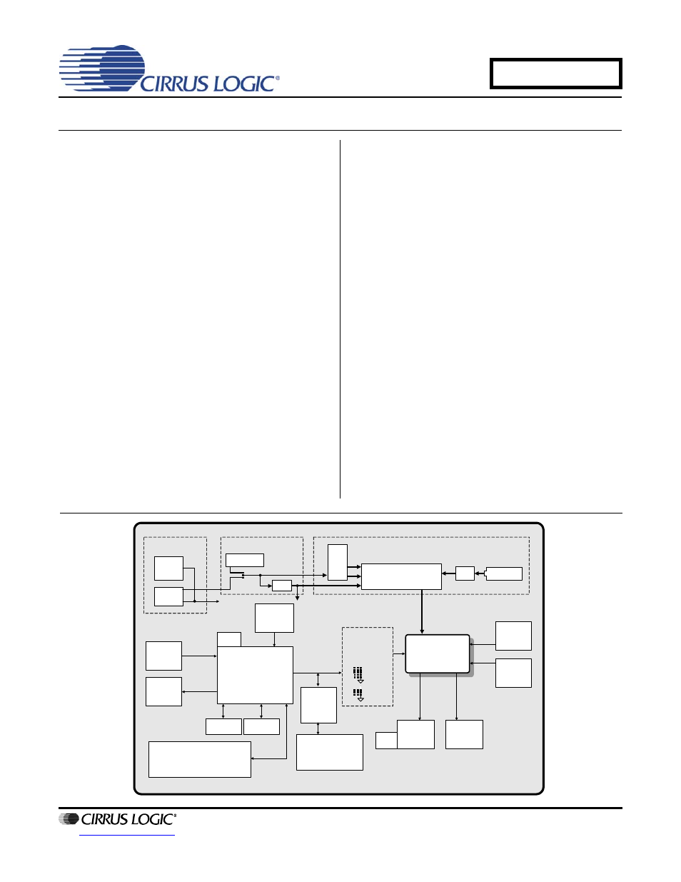
The CDB42L55 is the ideal evaluation platform solution to test
and evaluate the CS42L55.The CS42L55 is a highly integrat-
ed, 24-bit, ultra-low-power stereo CODEC based on multi-bit
Delta-Sigma modulation suitable for low-power portable sys-
tem applications. Use of the board requires an analog or digi-
tal signal source, an analyzer, and power supplies. A
Windows PC-compatible computer is also needed in order to
configure the CS42L55 and the board.
System timing can be provided by the CS8416 S/PDIF Re-
ceiver, by the CS42L55 supplied with a master clock, or via an
I/O stake header with a DSP connected.
RCA connectors are provided for CS42L55 analog inputs and
HP/Line outputs. A 1/8 inch audio jack is provided for head-
phone stereo out. Digital I/O connections are available via
RCA phono or optical connectors to the CS8416 and CS8406
(S/PDIF Rx and Tx).
The CDB42L55 is programmed via the PC’s USB using Cirrus
Logic’s Microsoft
®
Windows
®
-based FlexGUI software. The
evaluation board may also be configured to accept external
timing and data signals for operation in a user application dur-
ing system development.
Ordering Information
CDB42L55
Evaluation Board
USB
Serial
PC Control
Board Power
External 5.0 V
Supply
LDO’s
Buck
(not included)
1.8 V
2.5 V
3.3 V
1.8 V
CS42L55
FPGA
24 MHz
Oscillator
Clock/Data Routing
Clock dividers and PLL used
to derive all applicable Fs
from 24 MHz oscillator
PLL
I²C for all
applicable
devices
LDO
VL, VCP, VLDO, VA
MUX
3.3 V (VL only)
Circuit Break for
External System
Interface
PCM
Clocks/Data
I²C Clocks/
Data
I/O Stake Headers for Audio
Precision’s Programmable Serial
Interface Adapter (PSIA)
I/O SMA Connectors
for External System
Interface
Tri-state
Buffers
SRC (Rx)
SRC (Tx)
S/PDIF Rx
S/PDIF Tx
Stereo
Input 1
Stereo
Input 2
Stereo HP
Output
Stereo Line
Output
HP
Jack
x3
AAA Alkaline
CODEC Power
DEC '08
DS773DB1
CDB42L55
Document Outline
- Table of Contents
- List of Figures
- List of Tables
- 1 Quick Start Guide
- 2 System Overview
- 3 Configuration Options
- 4 Software Mode Control
- 5 System Connections and Jumpers
- 6 Performance Plots
- 7 CDB42L55 Block Diagram
- 8 CDB42L55 Schematics
- 9 CDB42L55 Layout
- 10 Revision History