2 jumper pin blocks, 3 test points, 2 jumper pin blocks 6.3 test points – Cirrus Logic CDB4244 User Manual
Page 21: Table 4. jumper pin blocks, Expla, S. see, Note 7, Note 8, Note 9, Cdb4244
DS900DB2
21
CDB4244
7.
Silk-screen labels are placed near these connectors to indicate the phase reversal between the active
(“A”) and passive (“P”) configurations. See
for more information.
8.
When using an optional single-ended output filter, the single pin labelled “+” and “-” under the “A” and
“P” columns respectively is ignored. This connectivity is shown in
9.
These connectors are intended for use with one of the optional single-ended output filters and are not
used by default. Refer to
for more information.
6.2
Jumper Pin Blocks
Notes:
10. See the CS4244 data sheet for performance differences between VA supply levels.
11. J63 and J64 must be closed during normal operation.
6.3
Test Points
The CDB4244 contains several convenient test points for analyzing signals to and from the CS4244. A
looped test point is available for each digital signal of the device’s control port and audio serial port, adjacent
to the respective external connection headers (J1 and J2, described in
). These test
points are connected directly to the appropriate CS4244 pins and can be used both with external control
(through the use of J1 and J2), or normal operation (J1 and J2 configured as described in
Test points are available for analog signals as well. The three-pin headers described in
serve as breakouts to allow access to the raw analog input signals, or filtered analog output signals. Fur-
thermore, two-pin headers (J41–J48) are available to observe the analog input and output pins of the
CS4244.
Note:
Headers J41–J48 should not be shunted. They are test points that have been designed using head-
ers to simplify layout.
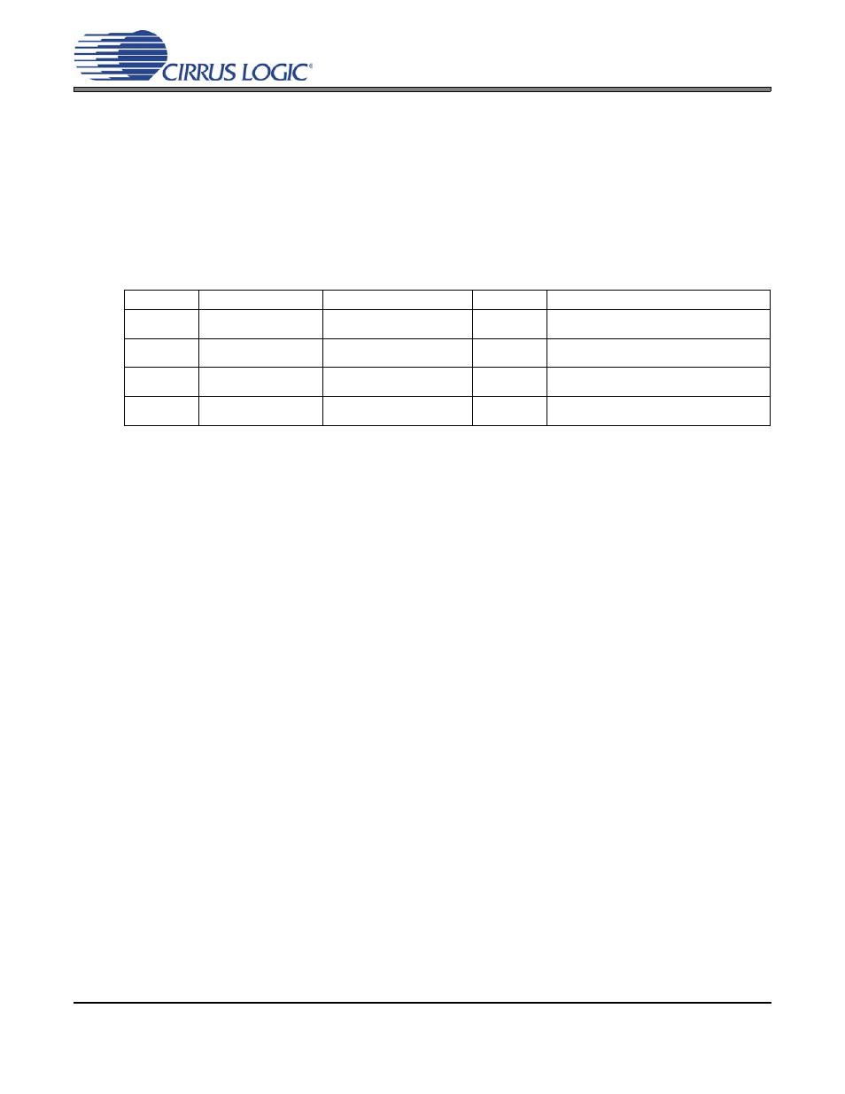
Label
Ref. Designator
Purpose
Position
Function Selected
+5V Select
J62
Selects +5-V voltage source.
POST*
USB
Voltage source is +5 V EXT binding post.
Voltage source is USB.
VA Select
J61
Selects VA voltage source.
See
+5V
+3.3V*
VA is +5 V.
VA is +3.3 V.
VA Current
J63
VA supply current measure-
ment.
Open
Closed*
1-
Ω resistor placed in series in supply path.
1-
Ω resistor is shorted. See
VL Current
J64
VL supply current measure-
ment.
Open
Closed*
1-
Ω resistor placed in series in supply path.
1-
Ω resistor is shorted. See
*Default factory setting
Table 4. Jumper Pin Blocks