An241 – Cirrus Logic AN241 User Manual
Page 9
AN241
9
the input sampling rate of the converter. Also, low value resistors should be used to minimize the addition
of resistor thermal noise.
Figure 4 implements a common mode capacitor between the analog input and the associated reference
voltage pin on each channel of the converter. This capacitor is commonly referred to as the anti-aliasing
capacitor, and performs several functions. The value of the capacitor affects the overall low pass filter re-
sponse and the amount of attenuation at the input sample rate of the converter. This capacitor also acts
as a charge reservoir for the internal sampling capacitors. Since this capacitor is located in the signal path,
it is very important not to use capacitors with a large voltage coefficient (such as general purpose ceram-
ics) since they can degrade signal linearity.
4.5
Recommended Filter Topology #2
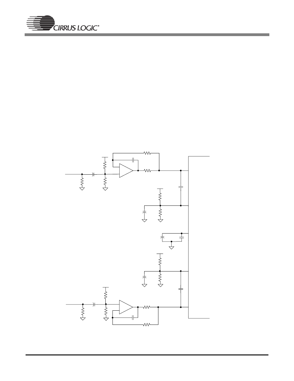
Figure 5 shows a single-ended analog input buffer with dedicated reference pins. This filter implements
one op-amp per channel, and uses passive components to properly bias the analog inputs and indepen-
dent channel reference pins. This buffer provides proper biasing, isolation from the switched capacitor
currents, low output impedance, and anti-alias filtering.
Figure 5. Single-Ended Input Buffer with Dedicated Reference Pins (Example #2)
AINL
VQ
in_left
VQ
out
-
+
470 pF
C0G
CSxxxx
634
Ω
91
Ω
2700 pF
C0G
4.7
µF
R k
Ω
1
µF
0.01
µF
AINR
2700 pF
C0G
-
+
470 pF
C0G
91
Ω
634
Ω
VQ
in_right
100 k
Ω
100 k
Ω
VA
4.7
µF
R k
Ω
100 k
Ω
100 k
Ω
VA
R k
Ω
100 k
Ω
VA
4.7
µF
R k
Ω
100 k
Ω
4.7
µF
VA