An241 – Cirrus Logic AN241 User Manual
Page 2
AN241
2
In the above example, the full scale input voltage is 5.64 Vpp (differentially), with each leg swinging
2.82 Vpp. Please note that the full scale input voltage level may vary from part to part. Also, the common
mode level (which in the above example is 2.5 0V) can also vary depending on the converter.
2.3
Recommended Filter Topology
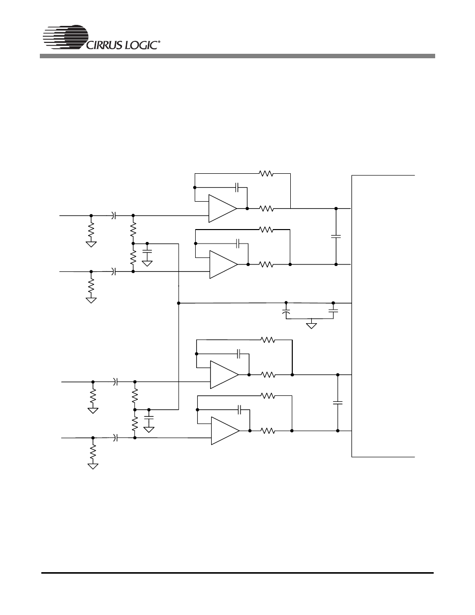
Figure 2 shows a fully differential analog input buffer. This buffer provides proper biasing, isolation from
the switched capacitor currents, low output impedance, and anti-alias filtering. The noise contribution of
this buffer is determined primarily by the noise floor of the op-amp.
Figure 2. Fully Differential Input Buffer
2.4
Overview of the Filter Topology
2.4.1
High Pass Filter and DC Biasing
The first stage of the buffer forms a high pass filter and provides the proper biasing to the positive termi-
nals of the op-amps. The high pass filter is formed from the combination of the AC-coupling capacitor
along with the resistor to the bias voltage reference (VQ or VCOM, depending on the naming convention).
The 3 dB corner of the high pass filter can be calculated as follows:
AIN+
AIN-
VQ or
VCOM
-
+
-
+
470 pF
C0G
470 pF
C0G
CSxxxx
634 Ω
91 Ω
634 Ω
91 Ω
2700 pF
C0G
10 µF
10 µF
10 kΩ
10 kΩ
0.01 µF
1 µF
0.01 µF
100 kΩ
100 kΩ
-
+
-
470 pF
C0G
470 pF
C0G
634 Ω
91 Ω
634 Ω
91 Ω
2700 pF
C0G
10 µF
10 kΩ
10 kΩ
0.01 µF
100 kΩ
AIN+
AIN-
100 kΩ
10 µF
+
-