An241 – Cirrus Logic AN241 User Manual
Page 14
AN241
14
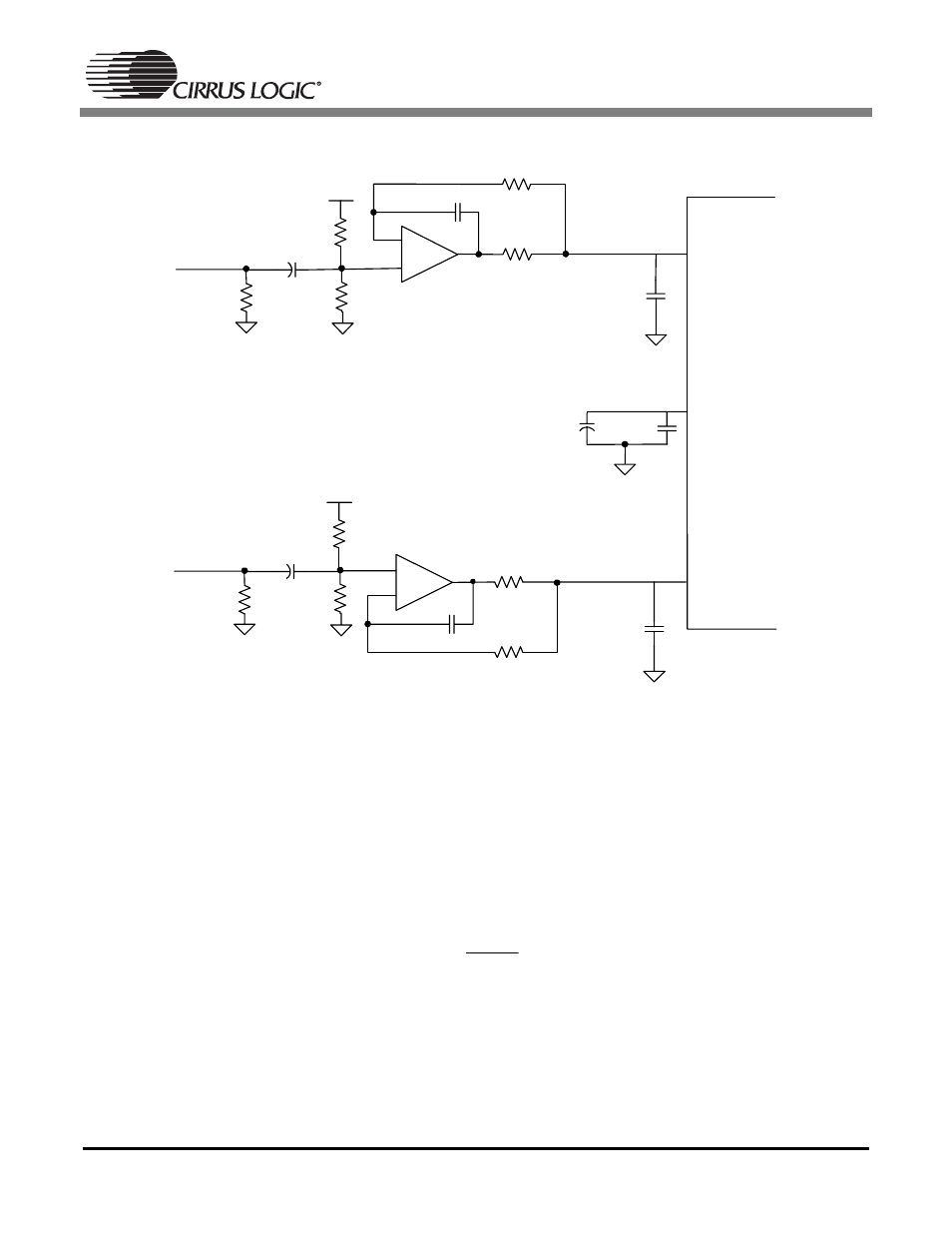
Figure 7. Single Ended Input Buffer with a Common Reference Pin
5.4
Overview of Filter Topology
5.4.1
High Pass Filter and DC Biasing
The first stage of the buffer forms a high pass filter from the combination of the AC-coupling capacitor
along with the resistor divider that biases the positive terminal of the op-amps to the proper DC bias volt-
age. The value of the resistors denoted as “R” will vary depending on the optimal DC bias for the given
converter. Typically this is around half of the VA voltage supply. Please refer to the converter datasheet
for the recommended input bias voltage. The 3dB corner of the high pass filter can be calculated as fol-
lows:
where:
R
EQ
is the value of the resistor divider in parallel (in Ohms)
C
is the value of the AC-coupling capacitor (in Farads)
AINL
VCOM
or V
Q
-
+
470 pF
C0G
CSxxxx
634 Ω
91 Ω
2700 pF
C0G
4.7 µF
R kΩ
1 µF
0.01 µF
AINR
2700 pF
C0G
-
+
470 pF
C0G
91 Ω
634 Ω
100 kΩ
100 kΩ
VA
4.7 µF
R kΩ
100 kΩ
100 kΩ
VA
C
R
F
EQ
C
π
2
1
=
- CobraNet (147 pages)
- CS4961xx (54 pages)
- CS150x (8 pages)
- CS1501 (16 pages)
- CS1601 (2 pages)
- CS1601 (16 pages)
- CS1610 (16 pages)
- CRD1610-8W (24 pages)
- CRD1611-8W (25 pages)
- CDB1610-8W (21 pages)
- CS1610A (18 pages)
- CDB1611-8W (21 pages)
- CDB1610A-8W (21 pages)
- CDB1611A-8W (21 pages)
- CRD1610A-8W (24 pages)
- CRD1611A-8W (25 pages)
- CS1615 (16 pages)
- AN403 (15 pages)
- AN401 (14 pages)
- AN400 (15 pages)
- AN375 (27 pages)
- AN376 (9 pages)
- CRD1615-8W (22 pages)
- CRD1616-8W (23 pages)
- AN402 (14 pages)
- AN404 (15 pages)
- CRD1615A-8W (21 pages)
- CS1615A (16 pages)
- CS1630 (56 pages)
- AN374 (35 pages)
- AN368 (80 pages)
- CRD1630-10W (24 pages)
- CRD1631-10W (25 pages)
- CS1680 (16 pages)
- AN405 (13 pages)
- AN379 (31 pages)
- CRD1680-7W (31 pages)
- AN335 (10 pages)
- AN334 (6 pages)
- AN312 (14 pages)
- AN Integrating CobraNet into Audio Products (16 pages)
- CobraNet Audio Routing Primer (9 pages)
- Bundle Assignments in CobraNet Systems (3 pages)
- CS2300-01 (3 pages)
- CS2000-CP (38 pages)