An241, Rg gain 634 1 – Cirrus Logic AN241 User Manual
Page 11
AN241
11
the converter is susceptible to aliasing). The characteristics of this low pass filter can be changed by ad-
justing the values of the resistors and capacitors in the feedback loop. However, it is important to maintain
a flat frequency response throughout the passband of interest and to provide reasonable attenuation at
the modulator sampling rate of the converter. Also, low value resistors should be used to minimize the
addition of resistor thermal noise.
Figure 5 implements a common mode capacitor between the analog input and the associated reference
voltage pin on each channel of the converter. This capacitor is commonly referred to as the anti-aliasing
capacitor, and performs several functions. The value of the capacitor affects the overall low pass filter re-
sponse and the amount of attenuation at the input sample rate of the converter. This capacitor also acts
as a charge reservoir for the internal sampling capacitors. Since this capacitor is located in the signal path,
it is very important not to use capacitors with a large voltage coefficient (such as general purpose ceram-
ics) since they can degrade signal linearity.
4.7
Recommended Filter Topology #3
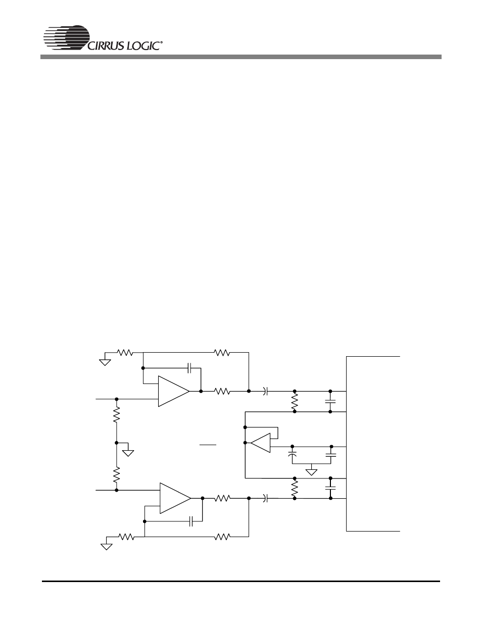
Figure 6 shows a single-ended analog input buffer with dedicated reference pins. This filter implements
one op-amp per channel, and uses a third op-amp to properly bias the independent channel reference
pins. This input buffer topology offers some unique advantages. First, the analog inputs to the op-amps
do not need to be AC-coupled (although they can be), which allows the input impedance of the buffer to
be set without regard to any charge up times. This can also be advantageous if the op-amps are restricted
to limited supply rails of
±
5 V. In this case, it is optimal to have an input referenced to ground in order to
prevent the op-amp from clipping. Secondly, this input buffer topology allows for some signal gain, as de-
termined by the resistor R
g
. Finally, this buffer provides proper biasing, isolation from the switched capac-
itor currents, and anti-alias filtering. On disadvantage of this topology is the large AC-coupling capacitor
directly on the input sampling node. The ESR of the capacitor will increase distortion, especially at low
frequencies where the ESR of the capacitor is generally much greater.
Figure 6. Single-Ended Input Buffer with Dedicated Reference Pins (Example #3)
AINL
VQ
in_left
VQ
out
-
+
470 pF
C0G
CSxxxx
634
Ω
91
Ω
2700 pF
C0G
10 k
Ω
10 k
Ω
1
µ
F
0.01
µ
F
AINR
2700 pF
C0G
-
+
470 pF
C0G
91
Ω
634
Ω
-
+
VQ
in_right
470
µ
F
470
µ
F
Rg
Rg
+
=
Rg
Gain
634
1
100 k
Ω
100 k
Ω