Cirrus Logic AN241 User Manual
An241 analog input buffer architectures

1
Copyright
Cirrus Logic, Inc. 2003
(All Rights Reserved)
http://www.cirrus.com
AN241
Analog Input Buffer Architectures
by Kevin L Tretter
1. Introduction
There are many considerations that must be taken into account when designing and implementing an an-
alog input buffer. These include negligible noise contribution, input biasing, isolation from switched ca-
pacitor currents, maintaining a low output impedance so as not to cause distortion, and providing anti-
alias filtering appropriate for the modulator sampling rate.
This application note provides several filter topologies that address the above concerns. The following an-
alog input buffers have been divided into four categories: fully differential, single-ended to differential, sin-
gle-ended with dedicated reference pins for each channel, and single-ended with a common, or shared,
reference.
2. Fully Differential Analog Input Buffer
2.1
Applicable Converters
A fully differential analog input buffer is ideal for use with the following Cirrus Logic audio converters:
- CS5361
- CS5381
- CS4272
- CS42528/26/18/16
- CS42428/26/18/16
2.2
Introduction to Differential Signals
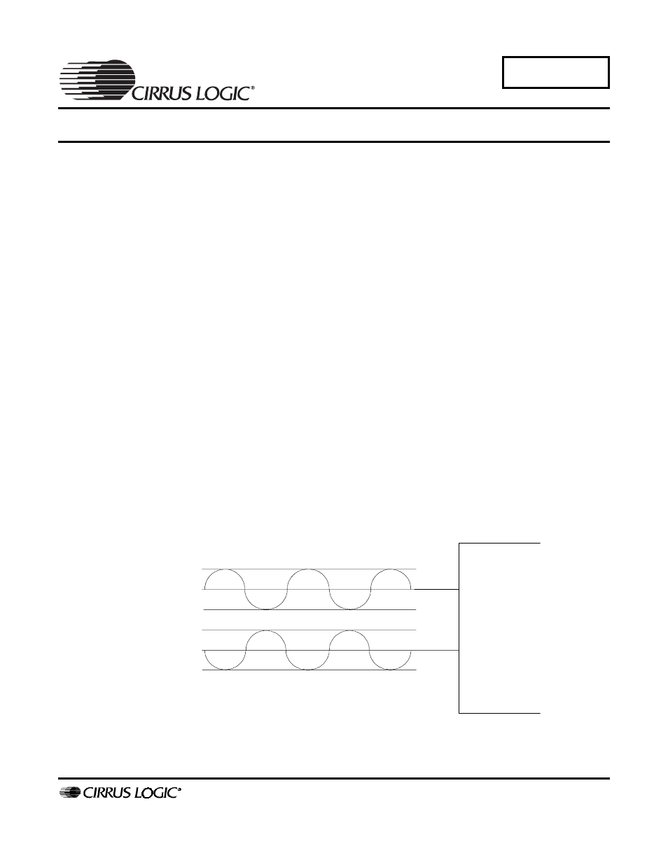
A differential signal can be defined as two nodes that have equal but opposite signals around a fixed point
(called the common mode level). The two signal nodes are typically referred to as positive and negative
(or non-inverting and inverting), as shown in the following example of a differential sine wave:
Figure 1. Example of a Differential Signal
CSxxxx
1.09 V
2.50 V
3.91 V
1.09 V
2.50 V
3.91 V
Full Scale Input Level = (AIN+) - (AIN-) = 5.64 Vpp
AIN+
AIN-
OCT ‘03
AN241REV1
