Ac electrical characteristics, Cs2100-cp – Cirrus Logic CS2100-CP User Manual
Page 7
CS2100-CP
DS840F2
7
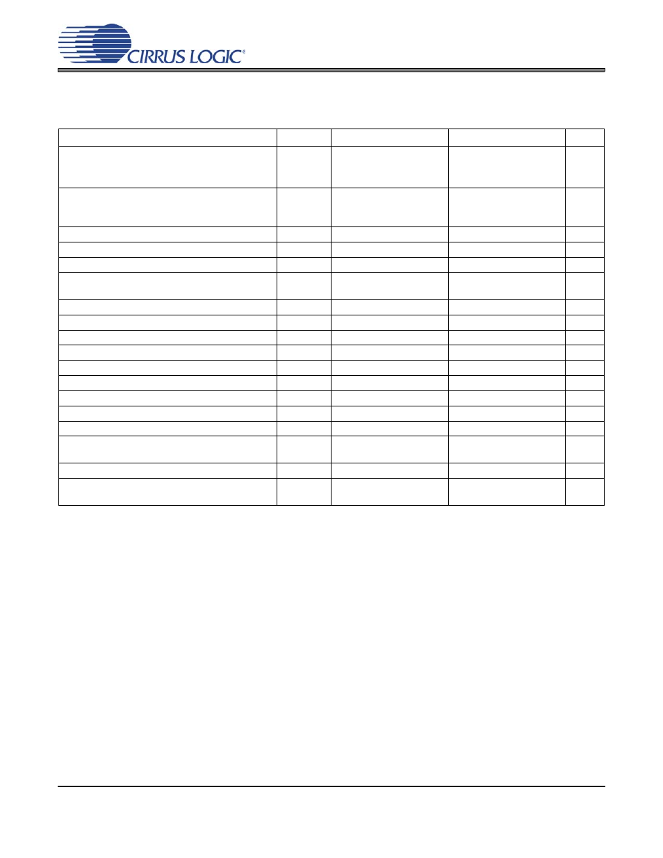
AC ELECTRICAL CHARACTERISTICS
Test Conditions (unless otherwise specified): VD = 3.1 V to 3.5 V; T
A
= -10°C to +70°C (Commercial Grade);
T
A
= -40°C to +85°C (Automotive Grade); C
L
= 15 pF.
Notes: 4.
1 UI (unit interval) corresponds to t
SYS_CLK
or 1/f
SYS_CLK
.
5.
t
CS
represents the time from the removal of CLK_IN by which CLK_IN must be re-applied to ensure that
PLL_OUT continues while the PLL re-acquires lock. This timeout is based on the internal VCO frequen-
cy, with the minimum timeout occurring at the maximum VCO frequency. Lower VCO frequencies will
result in larger values of t
CS
.
6.
Only valid in clock skipping mode; See
“CLK_IN Skipping Mode” on page 14
for more information.
7.
f
CLK_OUT
= 24.576 MHz; Sample size = 10,000 points; AuxOutSrc[1:0] = 11.
8.
In accordance with AES-12id-2006 section 3.4.2. Measurements are Time Interval Error taken with 3rd
order 100 Hz to 40 kHz bandpass filter.
9.
In accordance with AES-12id-2006 section 3.4.1. Measurements are Time Interval Error taken with 3rd
order 100 Hz Highpass filter.
10. 1 UI (unit interval) corresponds to t
CLK_IN
or 1/f
CLK_IN
.
11. The frequency accuracy of the PLL clock output is directly proportional to the frequency accuracy of the
reference clock.
Parameters
Symbol
Conditions
Min
Typ
Max
Units
Crystal Frequency
Fundamental Mode XTAL
f
XTAL
RefClkDiv[1:0] = 10
RefClkDiv[1:0] = 01
RefClkDiv[1:0] = 00
8
16
32
-
-
-
18.75
37.5
50
MHz
MHz
MHz
Reference Clock Input Frequency
f
REF_CLK
RefClkDiv[1:0] = 10
RefClkDiv[1:0] = 01
RefClkDiv[1:0] = 00
8
16
32
-
-
-
18.75
37.5
75
MHz
MHz
MHz
Reference Clock Input Duty Cycle
D
REF_CLK
45
-
55
%
Internal System Clock Frequency
f
SYS_CLK
8
18.75
MHz
Clock Input Frequency
f
CLK_IN
50 Hz
-
30
MHz
Clock Input Pulse Width (
Note 4
)
pw
CLK_IN
f
CLK_IN
< f
SYS_CLK
/96
f
CLK_IN
> f
SYS_CLK
/96
2
10
-
-
-
-
UI
ns
Clock Skipping Timeout
t
CS
,
6
)
20
-
-
ms
Clock Skipping Input Frequency
f
CLK_SKIP
(
Note 6
)
50 Hz
-
80
kHz
PLL Clock Output Frequency
f
CLK_OUT
6
-
75
MHz
PLL Clock Output Duty Cycle
t
OD
Measured at VD/2
45
50
55
%
Clock Output Rise Time
t
OR
20% to 80% of VD
-
1.7
3.0
ns
Clock Output Fall Time
t
OF
80% to 20% of VD
-
1.7
3.0
ns
Period Jitter
t
JIT
(
Note 7
)
-
70
-
ps rms
Base Band Jitter (100 Hz to 40 kHz)
(Notes
7
,
8
)
-
50
-
ps rms
Wide Band JItter (100 Hz Corner)
(Notes
7
,
9
)
-
175
-
ps rms
PLL Lock Time - CLK_IN (
Note 10
)
t
LC
f
CLK_IN
< 200 kHz
f
CLK_IN
> 200 kHz
-
-
100
1
200
3
UI
ms
PLL Lock Time - REF_CLK
t
LR
f
REF_CLK
= 8 to 75 MHz
-
1
3
ms
Output Frequency Synthesis Resolution (
Note 11
)
f
err
High Resolution
High Multiplication
0
0
-
-
±0.5
±112
ppm
ppm