Pin description, Cs2100-cp – Cirrus Logic CS2100-CP User Manual
Page 4
CS2100-CP
4
DS840F2
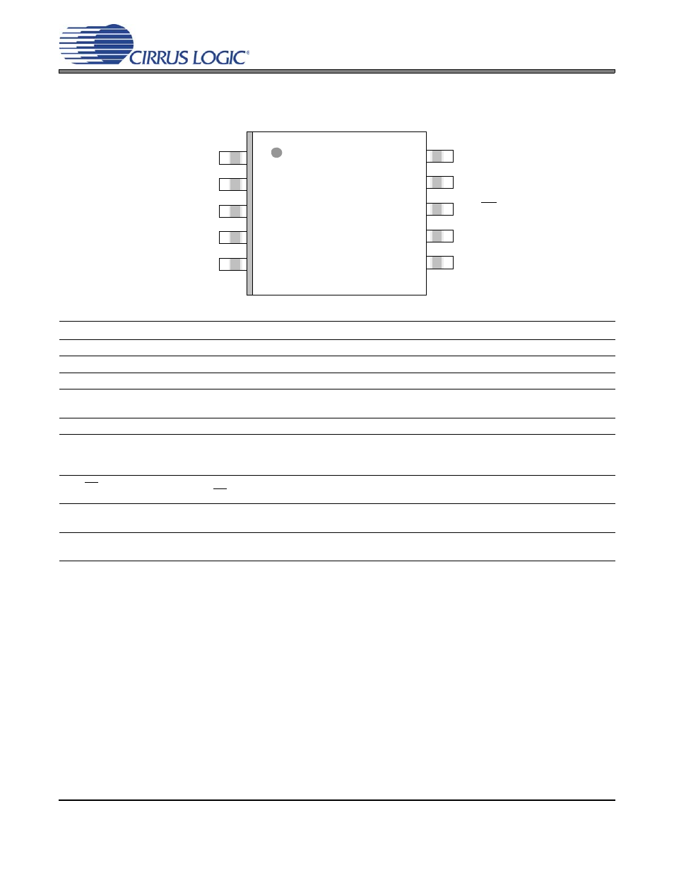
1. PIN DESCRIPTION
Pin Name
#
Pin Description
VD
1
Digital Power (Input) - Positive power supply for the digital and analog sections.
GND
2
Ground (Input) - Ground reference.
CLK_OUT
3
PLL Clock Output (Output) - PLL clock output.
AUX_OUT
4
Auxiliary Output (Output) - This pin outputs a buffered version of one of the input or output clocks,
or a status signal, depending on register configuration.
CLK_IN
5
Frequency Reference Clock Input (Input) - Clock input for the Digital PLL frequency reference.
XTO
XTI/REF_CLK
6
7
Crystal Connections (XTI/XTO) / Timing Reference Clock Input (REF_CLK) (Input/Output) -
XTI/XTO are I/O pins for an external crystal which may be used to generate the low-jitter PLL input
clock. REF_CLK is an input for an externally generated low-jitter reference clock.
AD0/CS
8
Address Bit 0 (I²C) / Control Port Chip Select (SPI) (Input) - AD0 is a chip address pin in I²C
Mode. CS is the chip select signal in SPI Mode.
SCL/CCLK
9
Control Port Clock (Input) - SCL/CCLK is the serial clock for the serial control port in I²C and SPI
mode.
SDA/CDIN
10
Serial Control Data (Input/Output) - SDA is the data I/O line in I²C Mode. CDIN is the input data
line for the control port interface in SPI Mode.
1
2
3
4
5
6
7
8
9
10
XTO
CLK_OUT
GND
VD
XTI/REF_CLK
AD0/CS
SCL/CCLK
SDA/CDIN
AUX_OUT
CLK_IN