6 function configuration 1 (address 16h), 1 clock skip enable (clkskipen), 2 aux pll lock output configuration (auxlockcfg) – Cirrus Logic CS2100-CP User Manual
Page 28: 3 reference clock input divider (refclkdiv[1:0]), P 28, Aux pll lock output config, Cs2100-cp
CS2100-CP
28
DS840F2
8.6
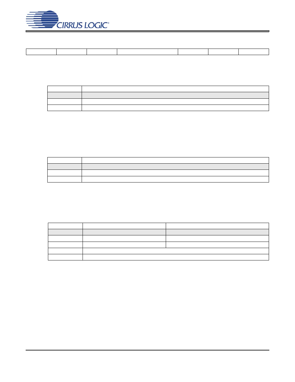
Function Configuration 1 (Address 16h)
8.6.1
Clock Skip Enable (ClkSkipEn)
This bit enables clock skipping mode for the PLL and allows the PLL to maintain lock even when the
CLK_IN has missing pulses.
Note:
f
CLK_IN
must be < 80 kHz and re-applied within
20
ms to use this feature.
8.6.2
AUX PLL Lock Output Configuration (AuxLockCfg)
When the AUX_OUT pin is configured as a lock indicator (AuxOutSrc[1:0] = 11), this bit configures the
AUX_OUT driver to either push-pull or open drain. It also determines the polarity of the lock signal. If
AUX_OUT is configured as a clock output, the state of this bit is disregarded.
Note:
AUX_OUT is an unlock indicator, signalling an error condition when the PLL is unlocked. There-
fore, the pin polarity is defined relative to the unlock condition.
8.6.3
Reference Clock Input Divider (RefClkDiv[1:0])
Selects the input divider for the timing reference clock.
7
6
5
4
3
2
1
0
ClkSkipEn
AuxLockCfg
Reserved
RefClkDiv1
RefClkDiv0
Reserved
Reserved
Reserved
ClkSkipEn
PLL Clock Skipping Mode
0
Disabled.
1
Enabled.
Application:
“CLK_IN Skipping Mode” on page 14
AuxLockCfg
AUX_OUT Driver Configuration
0
Push-Pull, Active High (output ‘high’ for unlocked condition, ‘low’ for locked condition).
1
Open Drain, Active Low (output ‘low’ for unlocked condition, high-Z for locked condition).
Application:
RefClkDiv[1:0]
Reference Clock Input Divider
REF_CLK Frequency Range
00
÷ 4.
32 MHz to 75 MHz (50 MHz with XTI)
01
÷ 2.
16 MHz to 37.5 MHz
10
÷ 1.
8 MHz to 18.75 MHz
11
Reserved.
Application:
“Internal Timing Reference Clock Divider” on page 13