3 output to input frequency ratio configuration, 1 user defined ratio (rud), 3 output – Cirrus Logic CS2100-CP User Manual
Page 17: Cs2100-cp, Pll bw = 1 hz, Pll bw = 128 hz
CS2100-CP
DS840F2
17
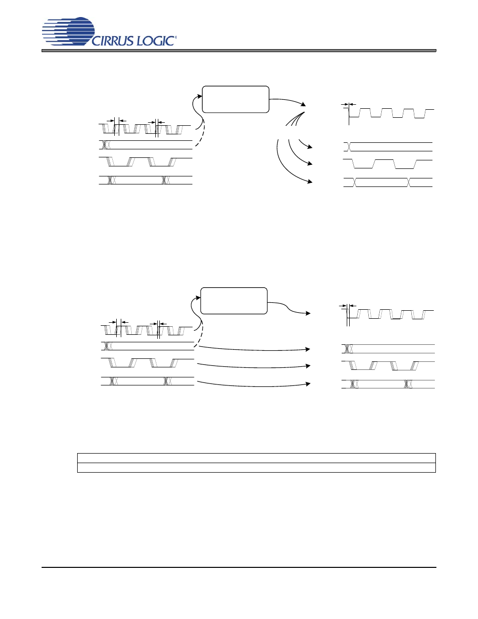
Typically, applications in which the PLL_OUT signal creates a new clock domain from which all other sys-
tem clocks and associated data are derived will benefit from the maximum jitter and wander rejection of
the lowest PLL bandwidth setting. See
.
Systems in which some clocks and data are derived from the PLL_OUT signal while other clocks and data
are derived from the CLK_IN signal will often require phase alignment of all the clocks and data in the
system. See
. If there is substantial wander on the CLK_IN signal in these applications, it may
be necessary to increase the minimum loop bandwidth allowing this wander to pass through to the
CLK_OUT signal in order to maintain phase alignment. For these applications, it is advised to experiment
with the loop bandwidth settings and choose the lowest bandwidth setting that does not produce system
timing errors due to wandering between the clocks and data synchronous to the CLK_IN domain and
those synchronous to the PLL_OUT domain.
It should be noted that manual adjustment of the minimum loop bandwidth is not necessary to acquire
lock; this adjustment is made automatically by the Digital PLL. While acquiring lock, the digital loop band-
width is automatically set to a large value. Once lock is achieved, the digital loop bandwidth will settle to
the minimum value selected by the ClkIn_BW[2:0] bits.
5.3
Output to Input Frequency Ratio Configuration
5.3.1
User Defined Ratio (R
UD
)
The User Defined Ratio, R
UD
, is a 32-bit un-signed fixed-point number, stored in the Ratio register set,
which determines the basis for the desired input to output clock ratio. The 32-bit R
UD
can be expressed
Referenced Control
Register Location
ClkIn_BW[2:0] .......................
“Clock Input Bandwidth (ClkIn_BW[2:0])” on page 29
Figure 15. Low bandwidth and new clock domain
LRCK
SCLK
SDATA
MCLK
MCLK
Wander > 1 Hz
Wander and Jitter > 1 Hz Rejected
D0
D1
LRCK
SCLK
SDATA
Subclocks generated
from new clock domain.
or
PLL
BW = 1 Hz
CLK_IN
PLL_OUT
D0
D1
Jitter
Figure 16. High bandwidth with CLK_IN domain re-use
D0
D1
LRCK
SCLK
SDATA
MCLK
MCLK
Wander < 128 Hz
Jitter > 128 Hz Rejected
Wander < 128 Hz Passed to Output
LRCK
SCLK
SDATA
or
PLL
BW = 128 Hz
CLK_IN
PLL_OUT
Subclocks and data re-used
from previous clock domain.
Jitter
D0
D1