4 com port pin 9 select – IEI Integration AFL-08B-N270 v2.30 User Manual
Page 34
AFL-08B-N270 User Manual
Page 34
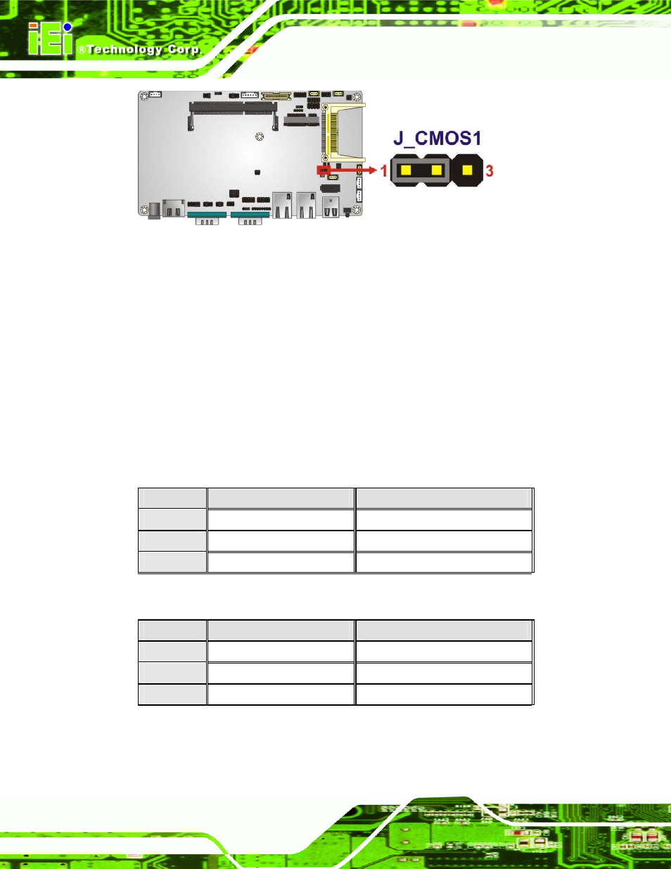
Figure 2-5: Clear CMOS Jumper
2.5.4 COM Port Pin 9 Select
Jumper Label:
JP8
and JP10
Jumper Settings:
See
5
Table 2-4
Jumper Location:
See
5
Figure 2-6
Two jumpers (JP8 and JP10) configure pin 9 on COM1 and COM3 DB-9 connectors. Pin 9
on the COM1 and the COM3 DB-9 connectors can be set as the ring (RI) signal, +5 V or
+12 V. The COM1 and COM3 Pin 9 Setting jumper selection options are shown in
5
Table
2-4
.
JP8
Description
Short 1-3
COM1 RI Pin use +12 V
Short 3-5
COM1 RI Pin use +5 V
Short 7-9
COM1 RI Pin use RI
Default
Table 2-4: COM1 Pin 9 Setting Jumper Settings
JP10
Description
Short 1-2
COM3 RI Pin use +12 V
Short 3-4
COM3 RI Pin use RI
Default
Short 5-6
COM3 RI Pin use +5 V
Table 2-5: COM3 Pin 9 Setting Jumper Settings
The COM1 and COM3 Pin 9 Setting jumper locations are shown in
5
Figure 2-6
below.
- UPC-V312-D525 v1.02 (176 pages)
- UPC-V312-D525 v1.10 (175 pages)
- UPC-12A_GM45 v1.00 (147 pages)
- UPC-12A_GM45 v2.00 (144 pages)
- UPC-12A_GM45 v2.10 (145 pages)
- UPC-V315-NM70 (148 pages)
- UPC-V315-Screw Driver (1 page)
- UPC-V315-QM77 (148 pages)
- S12ASR v1.12 (110 pages)
- S12ASR v3.00 (118 pages)
- PPC-5xxx-9455 v1.00 (198 pages)
- PPC-5xxx-9455 v1.10 (198 pages)
- PPC-WIDS-51xxA-G41 (152 pages)
- PPC-51xxA-H61 (193 pages)
- PPC-5152-D525 v1.02 (183 pages)
- PPC-5152-D525 v2.10 (185 pages)
- PPC-37xxA-N26 v1.00 (203 pages)
- PPC-37xxA-N26 v1.10 (200 pages)
- PPC-37xx-N270 v1.01 (165 pages)
- PPC-37xx-N270 v2.00 (155 pages)
- PPC-37xx-N270 v2.11 (155 pages)
- PPC-37xx-N270 v2.20 (162 pages)
- ACT-457A (67 pages)
- AFL-4 series-N270 v1.05 (165 pages)
- AFL-4 series-N270 v2.10 (166 pages)
- AFL-4 series-N270 v2.11 (168 pages)
- AFL-4 series-N270 v2.20 (168 pages)
- AFL-W19A_W19B_17D_W15A-GM45 v2.10 (138 pages)
- AFL-W19A_W19B_17D_W15A-GM45 v1.06 (138 pages)
- AFL-W19A_W19B_17D_W15A-GM45 v2.20 (151 pages)
- AFL-W15A_17D-GM45 v3.00 (148 pages)
- AFL-15i-HM55 v1.01 (139 pages)
- AFL-19i-HM55 v2.00 (140 pages)
- AFL-15i-HM55 v1.20 (143 pages)
- AFL-W19A_W19B_17D_W15A-N270 v1.06 (125 pages)
- AFL-W19A_W19B_17D_W15A-N270 v2.20 (124 pages)
- AFL-W19A_17D_W15A-N270 v3.00 (126 pages)
- AFL-15A_15AE-N270_UMN_v1.01.pdf (158 pages)
- AFL-15A-N270 v1.03 (159 pages)
- AFL-15A-N270 v2.10 (159 pages)
- AFL-15A-N270 v2.20 (158 pages)
- AFL-xxA-N26 (152 pages)
- AFL-xxA-N270-Series v1.03 (171 pages)
- AFL-xxA-N270-Series v2.00 (171 pages)
- AFL-xxA-N270-Series v2.11 (170 pages)