Solidtron, N-type semiconductor discharge switch, thinpak – Silicon Power CCS TA 43N40_N-Type Semiconductor Discharge Switch, ThinPak User Manual
Page 5
Packaging and Handling
1. ATTENTION OBSERVE PRECAUTIONS FOR HANDLING ELECTROSTATIC DISCHARGE
SENSITIVE DEVICES IN ALL ASSEMBLY AND TEST AREAS. Proper handling procedures must be
observed to prevent electrostatic discharge which may result in permanent damage to the device.
2. The CCSTA43N40 uses an undersized ceramic "lid" which exposes the sensitive Junction Termination
Extention (JTE) of the device. The user is required to encapsulate the device in an encapsulant prior to
applying high voltage. This prevents debris and contaminants from compromising the JTE.
2. Use of a seperate gate return path instead of the cathode power contact is recomended to minimize the
effects of rapidly changing Anode-Cathode currents.
3. Shorting resistor R
GK
is application specific. It can control the gate drive requirements and some device
properties. However, R
GK
= 10 Ohms satisfies most application requirements.
4. Installation reflow temperature should not exceed 260°C or internal package degradation may result.
T =125oC,
V
GE
=15V
T
C
=125
o
C, V
GE
=15V
Solidtron
TM
N-Type Semiconductor Discharge Switch, ThinPak
TM
CCSTA43N40A10
275 Great Valley Parkway
Malvern, PA 19355
Ph: 610-407-4700
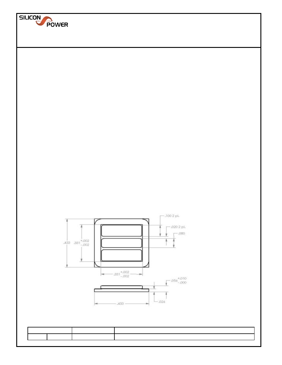
Dimensions
Revision History
Rev
EA #
0
04242009-NB-0016
Nature of Change
10-24-2007
Initial Issue
CAO 05/28/09
Date
CAO 05/28/09