Silicon Power SMCT AC 65N14_N-MOS VCS, Bare Die User Manual
Smctac65n16, Solidtron, N-mos vcs, bare die
Description
Package
Size - 6
The voltage controlled Solidtron
TM
(VCS) discharge switch is an n-
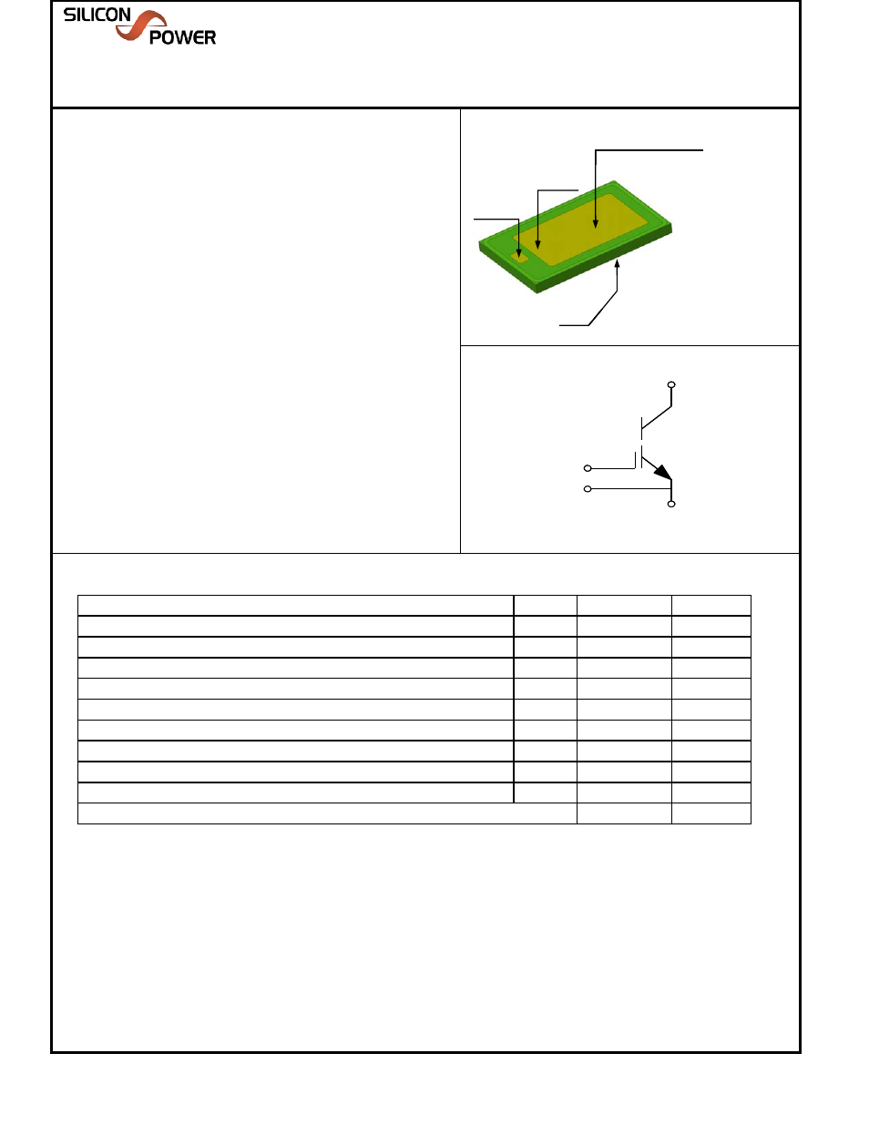
Cathode Bond Area
Solidtron
TM
N-MOS VCS, Bare Die
Data Sheet (Rev 0 - 10/28/10)
SMCTAC65N16
275 Great Valley Parkway
Malvern, PA 19355
Ph: 610-407-4700
Gate Bond
Area
Gate Return
Bond Area
The voltage controlled Solidtron
TM
(VCS) discharge switch is an n-
type MOS-Controlled Thyristor semiconductor.
The VCS features the high peak current capability and low On-
state voltage drop common to SCR thyristors combined with
extremely high dI/dt capability. This semiconductor is intended for
the control of high power circuits with the use of very small
amounts of input energy and is ideally suited for capacitor
discharge applications.
The cathode and gate contact pads are metallized with aluminum
for al min m ire bondable s rfaces
The Anode is metali ed
Cathode Bond Area
Solidtron
TM
N-MOS VCS, Bare Die
Data Sheet (Rev 0 - 10/28/10)
SMCTAC65N16
275 Great Valley Parkway
Malvern, PA 19355
Ph: 610-407-4700
Schematic Symbol
Gate Bond
Area
Gate Return
Bond Area
The voltage controlled Solidtron
TM
(VCS) discharge switch is an n-
type MOS-Controlled Thyristor semiconductor.
The VCS features the high peak current capability and low On-
state voltage drop common to SCR thyristors combined with
extremely high dI/dt capability. This semiconductor is intended for
the control of high power circuits with the use of very small
amounts of input energy and is ideally suited for capacitor
discharge applications.
The cathode and gate contact pads are metallized with aluminum
for aluminum wire bondable surfaces. The Anode is metalized
with solderable metal providing the user with a solderable die
attach device that may be installed using conventional or lead free
solders.
Anode (A)
Bare Die
Cathode Bond Area
Anode
Bond Area
Solidtron
TM
N-MOS VCS, Bare Die
Data Sheet (Rev 0 - 10/28/10)
SMCTAC65N16
275 Great Valley Parkway
Malvern, PA 19355
Ph: 610-407-4700
Features
Gate Bond
Area
Gate Return
Bond Area
The voltage controlled Solidtron
TM
(VCS) discharge switch is an n-
type MOS-Controlled Thyristor semiconductor.
The VCS features the high peak current capability and low On-
state voltage drop common to SCR thyristors combined with
extremely high dI/dt capability. This semiconductor is intended for
the control of high power circuits with the use of very small
amounts of input energy and is ideally suited for capacitor
discharge applications.
The cathode and gate contact pads are metallized with aluminum
for aluminum wire bondable surfaces. The Anode is metalized
with solderable metal providing the user with a solderable die
attach device that may be installed using conventional or lead free
solders.
1400V Peak Off-State Voltage
<150nSec Turn-On Delay
Low On-State Voltage
MOS Gated Control
Anode (A)
Gate (G)
Cathode (K)
Gate Return (GR)
Bare Die
Cathode Bond Area
Anode
Bond Area
Solidtron
TM
N-MOS VCS, Bare Die
Data Sheet (Rev 0 - 10/28/10)
SMCTAC65N16
275 Great Valley Parkway
Malvern, PA 19355
Ph: 610-407-4700
Absolute Maximum Ratings
SYMBOL
VALUE
UNITS
Peak Off-State Voltage
V
DRM
1400
V
Peak Reverse Voltage
V
RRM
-5
V
Off-State Rate of Change of Voltage Immunity
dv/dt
5000
V/uSec
Gate Bond
Area
Gate Return
Bond Area
The voltage controlled Solidtron
TM
(VCS) discharge switch is an n-
type MOS-Controlled Thyristor semiconductor.
The VCS features the high peak current capability and low On-
state voltage drop common to SCR thyristors combined with
extremely high dI/dt capability. This semiconductor is intended for
the control of high power circuits with the use of very small
amounts of input energy and is ideally suited for capacitor
discharge applications.
The cathode and gate contact pads are metallized with aluminum
for aluminum wire bondable surfaces. The Anode is metalized
with solderable metal providing the user with a solderable die
attach device that may be installed using conventional or lead free
solders.
1400V Peak Off-State Voltage
<150nSec Turn-On Delay
Low On-State Voltage
MOS Gated Control
Anode (A)
Gate (G)
Cathode (K)
Gate Return (GR)
Bare Die
Cathode Bond Area
Anode
Bond Area
Solidtron
TM
N-MOS VCS, Bare Die
Data Sheet (Rev 0 - 10/28/10)
SMCTAC65N16
275 Great Valley Parkway
Malvern, PA 19355
Ph: 610-407-4700
Continuous Anode Current at 110
o
C
I
A110
65
A
Repetitive Peak Anode Current (Pulse Width=1uSec)
I
ASM
6000
A
Rate of Change of Current
dI/dt
125
kA/uSec
Continuous Gate-Cathode Voltage
V
GKS
+/-20
V
Peak Gate-Cathode Voltage
V
GKM
+/-25
V
Minimum Negative Gate-Cathode Voltage Required for Garanteed Off-State
V
GK(OFF-MIN)
-5
V
M i
J
ti
T
t
T
150
o
C
Maximum Junction Temperature
T
JM
150
o
C
Maximum Soldering Temperature (Installation)
350
o
C