Silicon Power SMCT TA 32N14_N-MOS VCS, ThinPak User Manual
Solidtron, Thinpak, N-mos vcs, thinpak
Description
Package
Size - 4
Schematic Symbol
Features
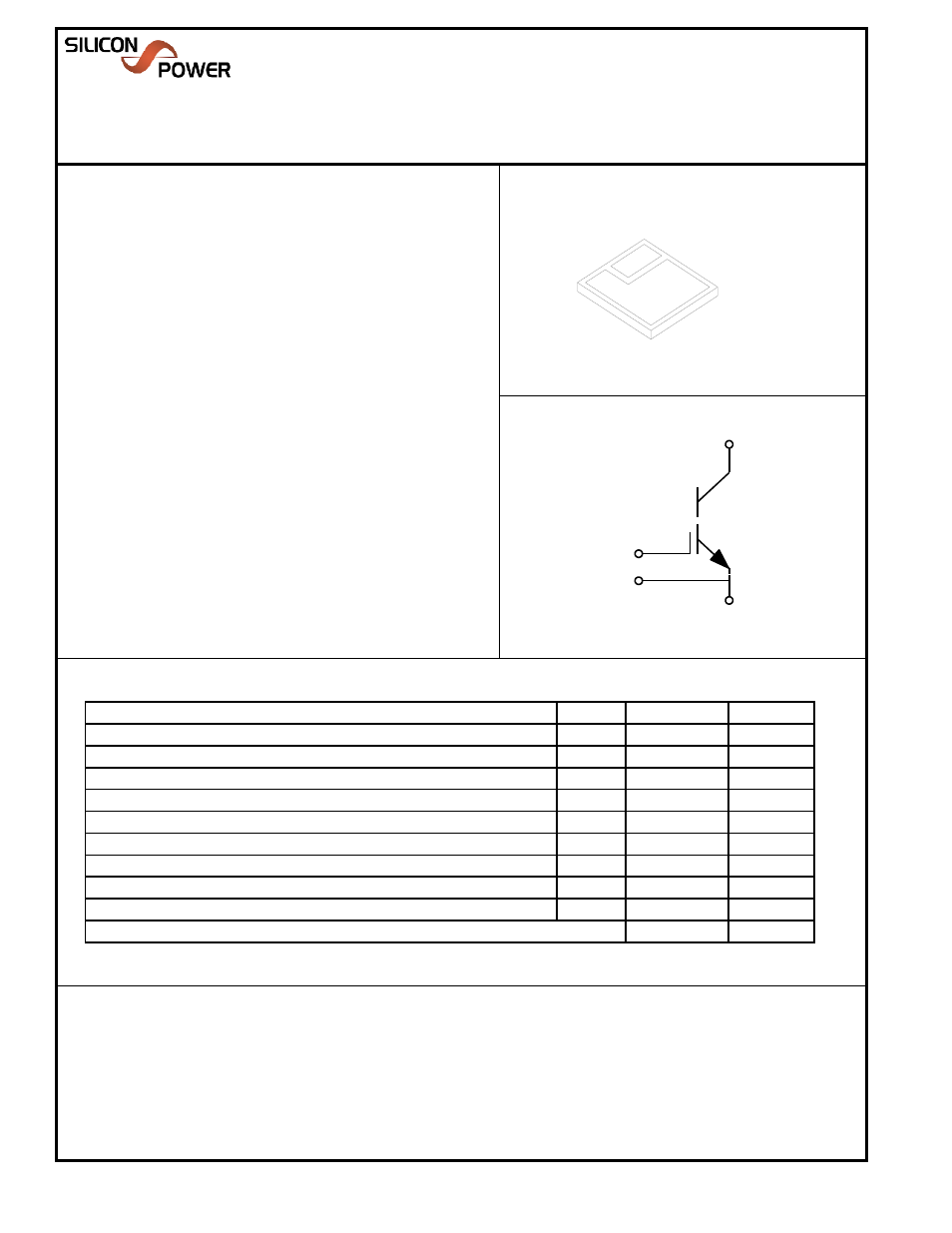
ThinPak
TM
Gate Bond Area
Gate Return
Anode
Cathode Bond Area
This voltage controlled Solidtron
TM
(VCS) discharge switch
utilizes an n-type MOS-Controlled Thyristor mounted on a
ThinPak
TM
, ceramic "chip-scale" hybrid.
The VCS features the high peak current capability and low On-
state voltage drop common to SCR thyristors combined with
extremely high dI/dt capability. This semiconductor is intended
for the control of high power circuits with the use of very small
amounts of input energy and is ideally suited for capacitor
discharge applications.
The ThinPak
TM
Package is a perforated, metalized ceramic
substrate attached to the silicon using 302
o
C solder. An epoxy
underfill is applied to protect the high voltage termination from
debris. All exterior metal surfaces are tinned with 63pb/37sn
solder providing the user with a circuit ready part. It's small size
and low profile make it extremely attractive to high dI/dt
applications where stray series inductance must be kept to a
minimum.
1400V Peak Off-State Voltage
32A Continuous Rating
<100nSec Turn-On Delay
Low On-State Voltage
Anode (A)
Gate (G)
Gate Return (GR)
SMCTTA32N14A10
275 Great Valley Parkway
Malvern, PA 19355
Ph: 610-407-4700
www.siliconpower.com
Solidtron
TM
N-MOS VCS, ThinPak
TM
Data Sheet (Rev 2 - 07/10/2008)
Absolute Maximum Ratings
SYMBOL
VALUE
UNITS
Peak Off-State Voltage
V
DRM
1400
V
Peak Reverse Voltage
V
RRM
-5
V
Off-State Rate of Change of Voltage Immunity
dv/dt
5000
V/uSec
Continuous Anode Current at 110
o
C
I
A110
32
A
Repetitive Peak Anode Current (Pulse Width=1uSec)
I
ASM
4000
A
Rate of Change of Current
dI/dt
120
kA/uSec
Continuous Gate-Cathode Voltage
V
GKS
+/-20
V
Peak Gate-Cathode Voltage
V
GKM
+/-25
V
Minimum Negative Gate-Cathode Voltage Required for Garanteed Off-State
V
GK(OFF-MIN)
-5
V
Maximum Junction Temperature
T
JM
150
o
C
Maximum Soldering Temperature (Installation)
260
o
C
This SILICON POWER product is protected by one or more of the following U.S. Patents:
CAO 05/28/09
5,446,316
5,557,656
5,564,226
5,517,058
4,814,283
5,135,890
5,521,436
5,585,310
5,248,901
5,366,932
5,497,013
5,532,635
5,105,536
5,777,346
5,446,316
5,577,656
5,473,193
5,166,773
5,209,390
5,139,972
5,103,290
5,028,987
5,304,847
5,569,957
4,958,211
5,111,268
5,260,590
5,350,935
5,640,300
5,184,206
5,206,186
5,757,036
5,777,346
5,995,349
4,801,985
4,476,671
4,857,983
4,888,627
4,912,541
5,424,563
5,399,892
5,468,668
5,082,795
4,980,741
4,941,026
4,927,772
4,739,387
4,648,174
4,644,637
4,374,389
4,750,666
4,429,011
5,293,070
32A Continuous Rating
4kA Surge Current Capability
>120kA/uSec dI/dt Capability
Low On-State Voltage
MOS Gated Control
Low Inductance Package
Cathode (K)
Gate Return (GR)
CAO 05/28/09