Solidtron – Silicon Power VCS FF 05N14_N-MOS VCS, F-Pak User Manual
Page 4
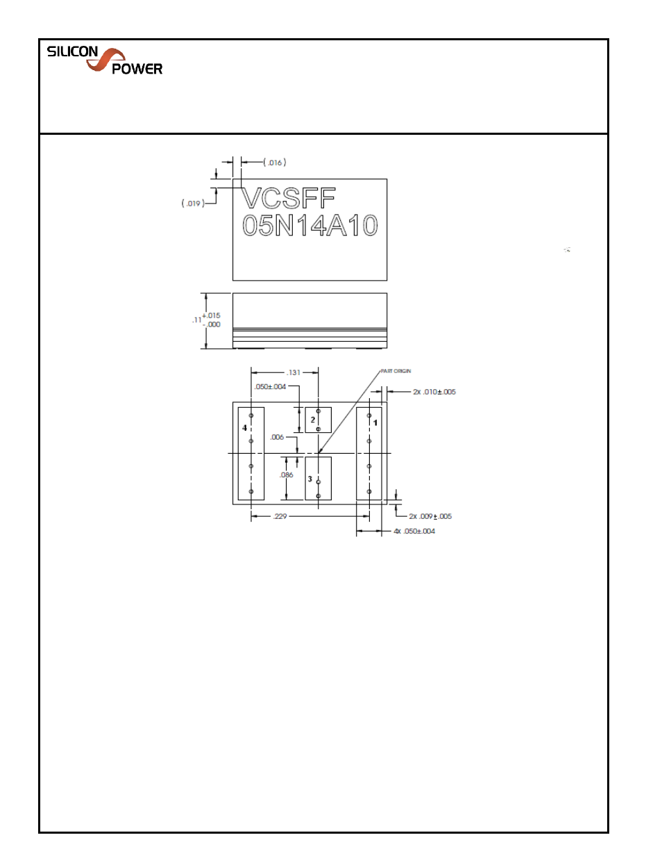
Package Dimensions
VCSFF05N14A10
Solidtron
TM
N-MOS VCS, F-Pak
Data Sheet (Rev 6- 06/17/11)
275 Great Valley Parkway
Malvern, PA 19355
Ph: 610-407-4700
fax: 610-407-3688
Figure 5. Critical Package Dimensions and Pin Assignment
Application Note:
All Dimensions are in inchs
Pins
1. Cathode
2. Gate
3. Gate Return
4. Anode
Use of Gate Return Bond Area.
The MCT was designed for high di/dt applications. An independent cathode connection or "Gate
Return Bond Area" was provided to minimize the effects of rapidly changing Anode‐Cathode
current on the Gate control voltage, (V=L*di/dt). It is therefore, critcal that the user utilize the
Gate Return Bond Area as the point at which the gate driver reference (return) is attached to the
VCS device.