Solidtron, N-mos vcs, f-pak, Is caculated using 1 / (f 2π) – Silicon Power VCS FF 05N14_N-MOS VCS, F-Pak User Manual
Page 3: C where f = frequency of i, See figure 4) •r
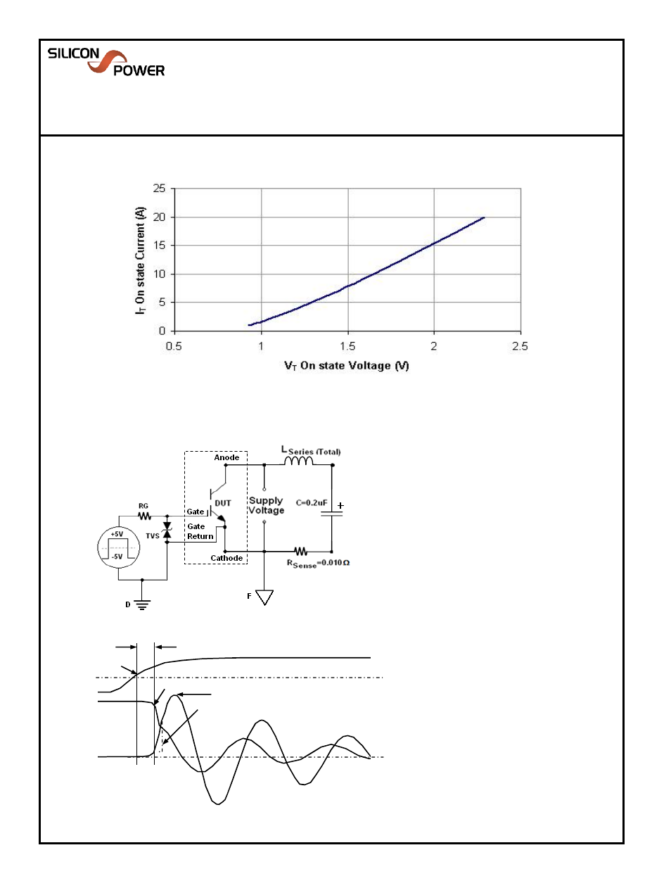
Typical Performance Curves (Continued)
Figure 2
On state characteristics
Test Circuit and Waveforms
VCSFF05N14A10
Solidtron
TM
N-MOS VCS, F-Pak
Data Sheet (Rev 6 - 06/17/11)
275 Great Valley Parkway
Malvern, PA 19355
Ph: 610-407-4700
fax: 610-407-3688
L
i
l t d
i
Figure 3. 0.16uF Pulsed Discharge Circuit Schematic
Figure 4. 0.16uF Pulsed Discharge Circuit Waveforms
V
GK
V
AK
I
A
I
P
T
DELAY(ON)
0 Ref.
0 Ref.
90%
10%
dI/dt - 10% to 50% of I
P
The waveform shown is
representative of one produced
using a very low inductance circuit
(<10nH).
V
GK
is held positive until I
A
oscillations have ended ( I
A
=0).
•L
SERIES(TOTAL)
is caculated using
1 / (f 2π)
2
C where
f = frequency of I
A
(See Figure 4)
•R
SENSE
is a calibrated
Current Viewing Resistor (CVR)
•TVS ‐ Fairchild SMBJ9V0CA
•Gate driver circuit ground connected to
GR (Gate Return) . Donot connect gate
circuit ground to cathode external to the
device.