Solidtron, N-mos vcs, bare-die – Silicon Power SMCT AC 05N14_N-MOS VCS, Bare-Die User Manual
Page 3
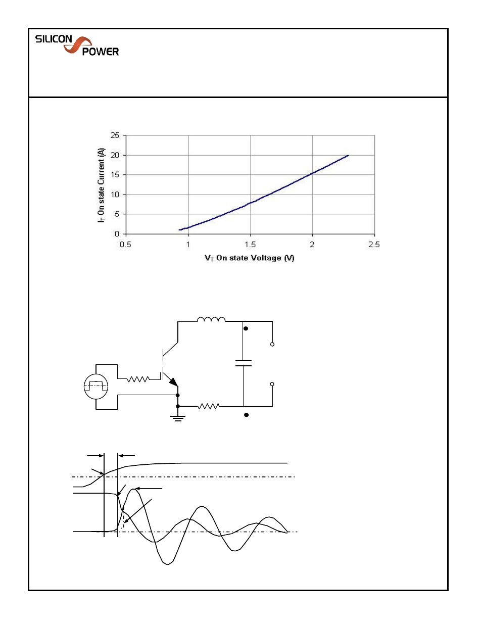
Typical Performance Curves (Continued)
Figure 2
On state characteristics
SMCTAC05N14A10
Solidtron
TM
N-MOS VCS, Bare-Die
Data Sheet (Rev 1 - 03/30/09)
275 Great Valley Parkway
Malvern, PA 19355
Ph: 610-407-4700
fax: 610-407-3688
Test Circuit and Waveforms
Figure 3. 0.16uF Pulsed Discharge Circuit Schematic
Figure 4. 0.16uF Pulsed Discharge Circuit Waveforms
CAO 05/28/09
V
GK
V
AK
I
A
I
P
T
DELAY(ON)
0 Ref.
0 Ref.
90%
10%
dI/dt - 10% to 50% of I
P
The waveform shown is
representative of one produced using a
very low inductance circuit (<10nH).
V
GK
is held positive until I
A
oscillations have ended ( I
A
=0).
Supply
Voltage
L
SERIES (TOTAL)
DUT
R
SENSE
= 0.010Ω
Ω
Ω
Ω
C=0.16uF
+
-
R
G
Gate
Driver
+5V
-5V
L
SERIES(TOTAL)
is calculated using
1 / (f 2π)
2
C
where f = frequency of I
A
(See Figure 4)
R
SENSE
is a calibrated
Current Viewing Resistor (CVR)
CAO 05/28/09