Encoder side, Driver side, Termination pinouts – BEI Sensors Encoder Signal Broadcaster Module User Manual
Page 3: Broadcaster block diagram
924-02097-001 Rev 3/09
Copyright 2009 by BEI Industrial Encoders, 1-800-ENCODER,
www.beiied.com
7230 Hollister Avenue, Goleta, California 93117-2807
Tel: 800-350-2727 Fax: 800-960-2726
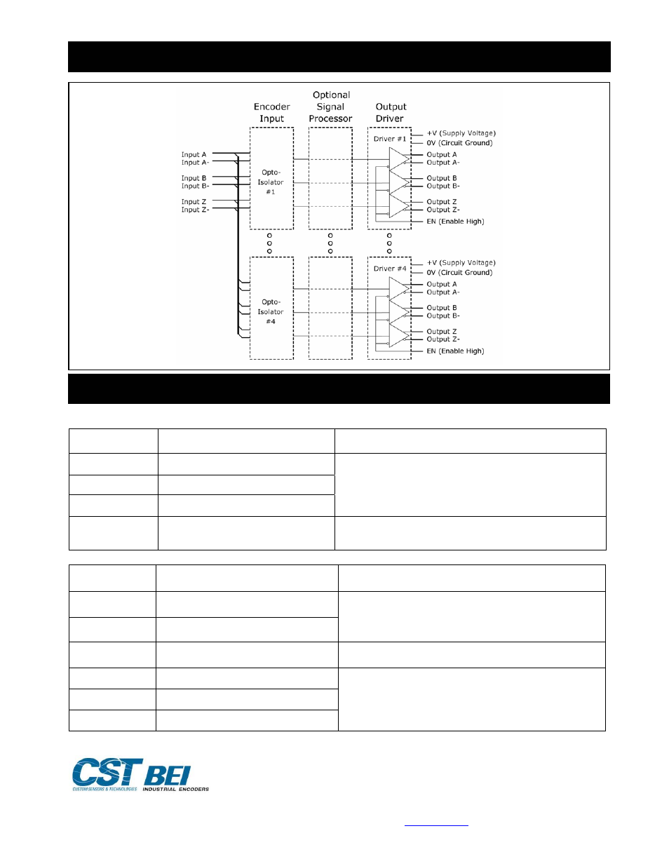
ENCODER SIDE
PIN DESCRIPTION
NOTES
A, A/
Channel A Inputs
B, B/
Channel B Inputs
Z, Z/
Channel Z Inputs
Input levels consistent with specified value in model
number (5 V, 15 V, 24 V).
Signal input current 25 mA nom.
See BEI OIM Applications Guide for single ended
and open collector connection diagrams
T1, T2, T3
Uncommitted Terminals
Non-committed terminals. Provided for use as
connection points for encoder power.
DRIVER SIDE
TERMINATION PINOUTS
BROADCASTER BLOCK DIAGRAM
PIN DESCRIPTION
NOTES
+ V
Power supply 5 – 28 VDC
125 mA + load current typ.
0 V
Power supply common
Supply lines between driver sections are not
connected. Driver must be powered in order to
produce an output. Supply voltage need not be the
same for different driver sections.
EN Output
Enable
HI = Output Active, LO = High Impedance Internal
pull-up to V+
A, A/
Channel A Outputs
B, B/
Channel B Outputs
Z, Z/
Channel Z Outputs
Output levels consistent with driver type and supply
voltage (V/V outputs).