Communication Concepts 2M-1KW 2 Meter 1KW Amplifier User Manual
Page 5
MRFE6VP61K25HR6 MRFE6VP61K25HSR6
5
RF Device Data
Freescale Semiconductor
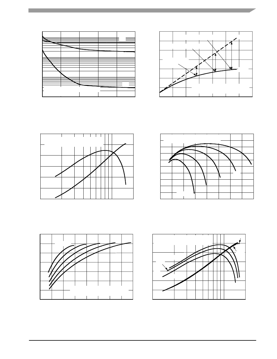
TYPICAL CHARACTERISTICS
50
10
2000
0
20
10
V
DS
, DRAIN--SOURCE VOLTAGE (VOLTS)
Figure 4. Capacitance versus Drain--Source Voltage
C,
CA
PA
CIT
ANCE
(pF
)
30
C
iss
1000
100
40
C
oss
Measured with ±30 mV(rms)ac @ 1 MHz
V
GS
= 0 Vdc
Note: Each side of device measured separately.
1
59
66
35
P
in
, INPUT POWER (dBm) PULSED
Figure 5. Pulsed Output Power versus
Input Power
64
36
37
38
39
40
41
42
P
out
,O
UT
PU
T
POWER
(d
Bm)
PU
LSED
63
60
Actual
Ideal
V
DD
= 50 Vdc, I
DQ
= 100 mA, f = 230 MHz
Pulse Width = 100 μsec, 20% Duty Cycle
P1dB = 61.3 dBm
(1333 W)
62
61
65
P3dB = 61.9 dBm (1553 W)
P2dB = 61.7 dBm (1472 W)
26
30
90
100
24
70
50
P
out
, OUTPUT POWER (WATTS) PULSED
Figure 6. Pulsed Power Gain and Drain Efficiency
versus Output Power
G
ps
,P
OWER
GAIN
(d
B)
η
D,
DRA
IN
EF
FI
CIE
NCY
(%
)
22
20
2000
21
40
60
80
23
25
16
23
0
20
19
P
out
, OUTPUT POWER (WATTS) PULSED
Figure 7. Pulsed Power Gain versus
Output Power
G
ps
,P
OWER
GAIN
(d
B)
200
18
1400 1600
V
DD
= 50 Vdc, I
DQ
= 100 mA, f = 230 MHz
Pulse Width = 100 μsec, 20% Duty Cycle
17
400
800
1000
1200
V
DD
= 30 V
50 V
21
22
25
24
26
600
35 V
40 V
45 V
20
90
0
P
out
, OUTPUT POWER (WATTS) PULSED
Figure 8. Pulsed Drain Efficiency versus
Output Power
70
200
400
600
800
1000
1200
1400
60
30
50
40
80
1600
Figure 9. Pulsed Power Gain and Drain Efficiency
versus Output Power
P
out
, OUTPUT POWER (WATTS) PULSED
G
ps
,P
OWER
GAIN
(d
B)
19
21
20
100
2000
η
D
25_C
T
C
= --30_C
85_C
G
ps
V
DD
= 50 Vdc, I
DQ
= 100 mA, f = 230 MHz
Pulse Width = 100 μsec, 20% Duty Cycle
40
60
50
20
30
η
D
,DRA
IN
EF
FI
CIE
NCY
(%
)
--30_C
25_C
85_C
V
DD
= 50 Vdc, I
DQ
= 100 mA, f = 230 MHz
Pulse Width = 100 μsec, 20% Duty Cycle
V
DD
= 30 V
50 V
35 V
40 V
45 V
η
D,
DRA
IN
EF
FI
CIE
NCY
(%
)
24
23
22
26
25
70
80
90
C
rss
1000
η
D
G
ps
V
DD
= 50 Vdc, I
DQ
= 100 mA, f = 230 MHz
Pulse Width = 100 μsec, 20% Duty Cycle
2000
1000