Communication Concepts 2M-1KW 2 Meter 1KW Amplifier User Manual
Page 3
MRFE6VP61K25HR6 MRFE6VP61K25HSR6
3
RF Device Data
Freescale Semiconductor
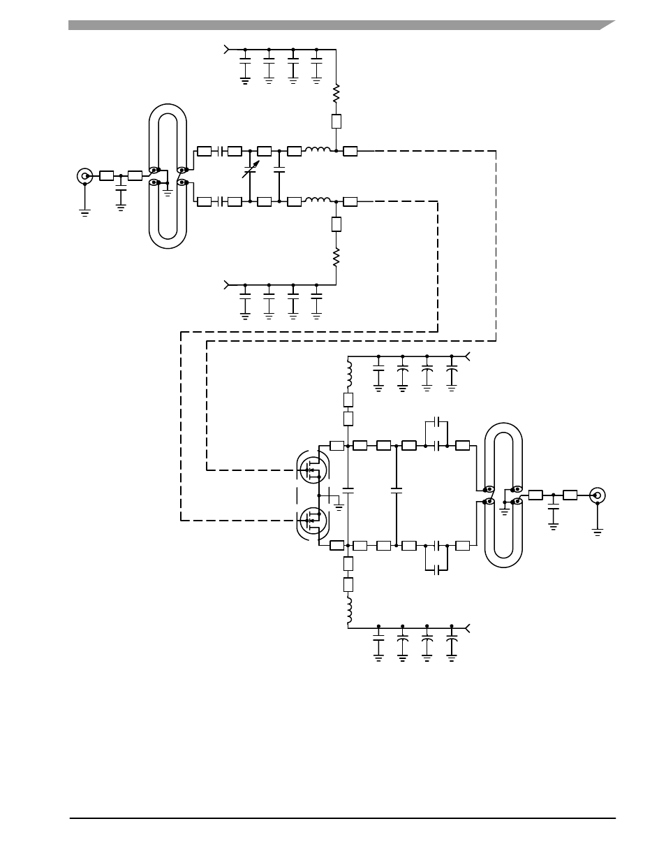
Figure 2. MRFE6VP61K25HR6(HSR6) Test Circuit Schematic — Pulsed
Z23, Z24
1.251″ x 0.300″ Microstrip
Z25, Z26
0.127″ x 0.300″ Microstrip
Z27, Z28
0.116″ x 0.300″ Microstrip
Z29
0.186″ x 0.082″ Microstrip
Z30
0.179″ x 0.082″ Microstrip
* Line length includes microstrip bends
Z1
0.192″ x 0.082″ Microstrip
Z2
0.175″ x 0.082″ Microstrip
Z3, Z4
0.170″ x 0.100″ Microstrip
Z5, Z6
0.116″ x 0.285″ Microstrip
Z7, Z8
0.116″ x 0.285″ Microstrip
Z9, Z10
0.108″ x 0.285″ Microstrip
RF
INPUT Z1
DUT
Z16
Z18
Z17
C16
C4
Z23
Z25
COAX1
COAX2
Z27
C10
+
L1
C17
C18
C19
Z28
Z26
C15
Z24
C1
Z11
C12
C11
C13
Z15
Z21
Z22
C14
V
BIAS
V
SUPPLY
C22
C23
+
C21
C24
+
L4
Z2
Z3
Z4
C2
C3
Z5
Z6
Z7
Z8
C5
Z9
Z10
L2
R1
Z12
R2
C6
+
C8
C7
C9
V
BIAS
Z13
Z14
Z20
Z19
L3
+
V
SUPPLY
C26
C27
+
C25
C28
+
+
C20
RF
OUTPUT
Z29
COAX3
COAX4
Z30
Z11*, Z12*
0.872″ x 0.058″ Microstrip
Z13, Z14
0.412″ x 0.726″ Microstrip
Z15, Z16
0.371″ x 0.507″ Microstrip
Z17*, Z18*
0.466″ x 0.363″ Microstrip
Z19*, Z20*
1.187″ x 0.154″ Microstrip
Z21, Z22
0.104″ x 0.507″ Microstrip